

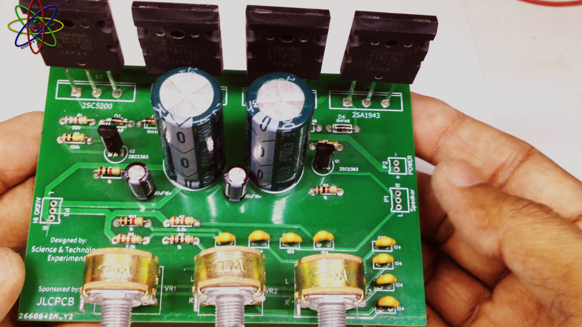
In the following video I showed, how to make a powerful C5200 A1943 Stereo Amplifier with heavy bass, treble and volume controllers. The high quality circuit uses minimum components with a low cost and ideal for beginners.
This video was sponsored by JLCPCB which is one of the largest PCB manufacturing company in China. You can download the gerber file of this project and can re-order it from the manufacturer. Link of which is already provided in the list of components at end of this article.

Circuit Diagram
of C5200 A1943 Stereo Amplifier
This is the circuit diagram of C5200 NPN & A1943 PNP transistors Stereo Amplifier including bass, treble and volume controllers. 2SC2383 NPN transistor is also used in pre-amplifier stage. The amplifier provides high bass and its ideal for bass lovers. You can click on the image to open it in a light box then click the “Download” button to download the circuit diagram into your computer’s disk.

More Circuit Layouts


Development Images
used in C5200 A1943 Stereo Amplifier
Following is the image of front side view of PCB extracted from gerber file. You can re-print the file or you can order it from JLCPCB for your own project. I have already provided a clickable link of gerber file at the end of this article in the list of components section.

Following image shows the rear view of PCB of this project. The PCB uses two layers in circuit which is attached each other internally. The stereo board is designed compact within 4 inch x 4 inch size which can be fit in small box and doesn’t require large space.

This following image shows the text layer. You can easily print on PCB through this image at home for making as DIY project.

This PCB is designed in 3 layers. You can see both upper and bottom layers at a glance in the following print.

JLCPCB company of China has delivered this package box via DHL shipment where I received 5 nos of PCB in just $2 and received within a week time.

In the following image, I soldered all components without 4 transistors and 2 large capacitors. All the holes and the space of each component is in perfect size. The finishing of the PCB is outstanding.

On this stage I have soldered all parts. I will just fix the heat sink. The heat sink should be large enough and thick for proper dissipation of heat of all transistors. The transistors heats up during running and it requires proper heat dissipation. Smaller heat sink can not cool the transistors properly which causes transistors burning.
List of components
used in C5200 A1943 Stereo Amplifier
- 2SC5200 transistor x 2
- 2SA1943 transistor x 2
- 2SC2383 transistor x 2
- 1N4148 diode x 4
- 4700uf capacitor x 2
- 220uf capacitor x 2
- 104 capacitor x 8
- 680 ohms / 1 watt resistor x 2
- 100k ohms resistor x 2
- 1k ohms resistor x 6
- 2.2k ohms resistor x 4
- 50k dual potentiometer x 3
- PCB x 1
- Heatsink x 1
- Power supply single 12v
- Speaker 4 ohms
- Download Gerber File
Thanks for watching and visiting the site. Please share it with your friends. Thanks.
You may also like:
 DIY C5200 stereo amplifier with volume balance
- C5200 Stereo Bass Amplifier DIY Volume Bass Treble
- TDA2030 DIY Powerful Amplifier with Volume Bass Treble
- DIY LA4440 bass amplifier homemade
- C5200 Bass Amplifier DIY Homemade with Volume
- 13003 amplifier DIY homemade dual transistor
- Modify PAM8403 Stereo Amplifier Board
- D718 amplifier heavy bass controller


hi how many amp for the power supply and what is wattage out put
12v-24v / 3A-5A / 100w
How to download the “Gerber File”?
how without tone control??
Hey the download link isn’t clickable!
Its working.
Gerber file link isn’t working, how do you download it?
Good day. Is it possible to make it to have two outputs of 50w max each?
Or its safe just to hook up two speakers to one output?
Guerber ????
The download link isn’t clickable!
como faço pra comprar esse amplificador
I can’t source 1N4148, 1N4149 or its equivalent fast switching diode, can I use 1N4004?
Yes you can. I’ve tried it. Confirm the polarities however.
I made it accordingly, but the sound is so quiet.
I have 12V DC powerr supply / 800 mA.
I have second amplifier on TDA7297 15W, and that’s one play ok, level of music is very high
I made it accordingly to tutorial, but level of sound is very low.
Why?