Introduction
Introducing the Stereo Amplifier TDA1552 DIY kit, a great way to kickstart any casual music project! This kit contains all the required components for building an excellent stereo amplifier. The board features robust circuitry and a high-quality power supply to ensure reliable performance no matter the application. Controls are straightforward and easy to understand, giving users access to adjust volume, balance, and even bass/treble adjustment. Included in the package is detailed documentation on how to assemble and get your amplifier up and running quickly. If you’re just starting out with electronics projects, this could be the perfect solution for you!
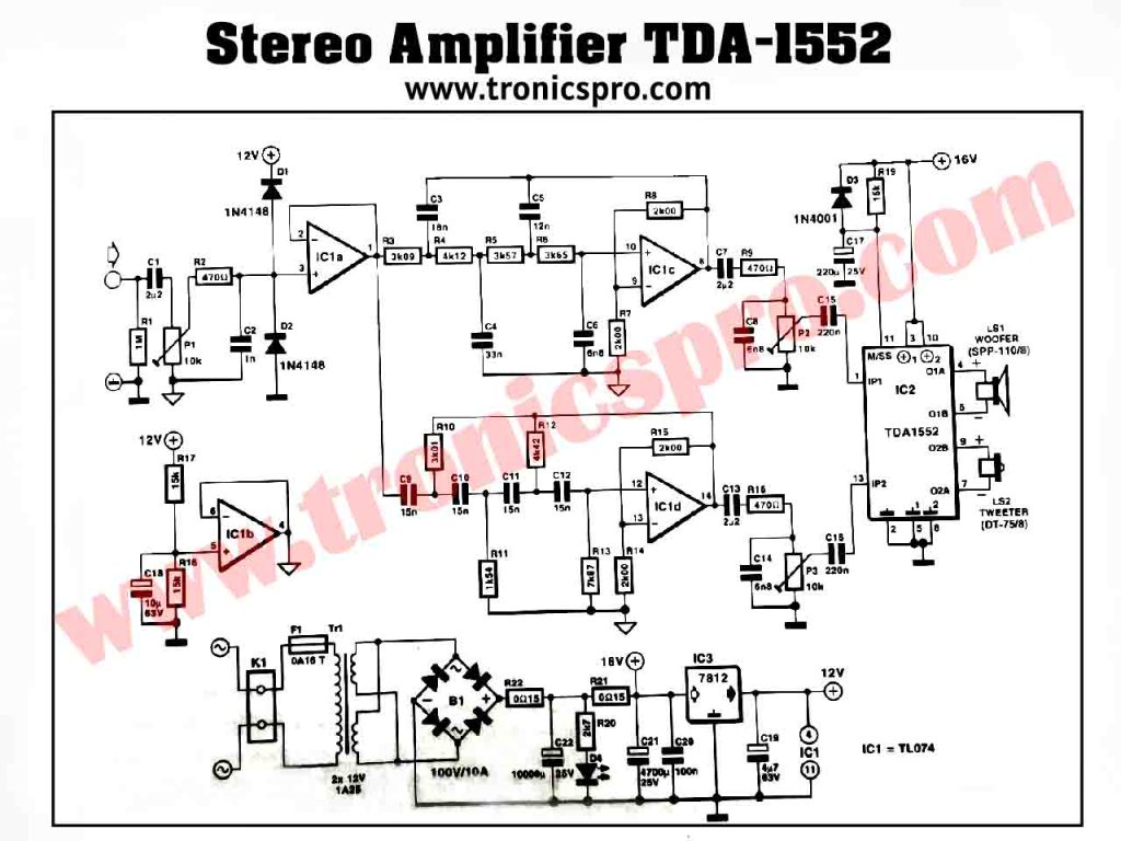
The Stereo Amplifier with TDA1552 DIY in this system may be used to drive the two-way loudspeaker. The overall system consists of an active two-way crossover network with a cut-off frequency of 3 kHz, a small output amplifier, and a power supply.
Circuit diagram
of Stereo Amplifier TDA1552 DIY
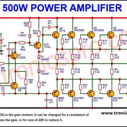
Building a DIY stereo amplifier using the TDA1552 circuit diagram is an excellent way to get great sound out of your audio system. It’s suitable for DIYers of all experience levels and allows you to configure your amplification to meet your personal needs. The circuit diagram itself is easy to follow, with its clear labeling of components and stages making sure that even beginners can build their own stereo amplifiers with confidence. Once built, it delivers exceptional sound quality with minimum distortion and impressive power handling capabilities – it could easily become the heart of a powerful home audio setup that you’ll enjoy for years to come.
More Circuit Layouts


Working Explanation
of Stereo Amplifier TDA1552 DIY
The output of stereo amplifier tda1552 DIY is based on a dual-integrated bridge amplifier, IC2, which was developed for use in cars. With a power supply voltage of 16 V, the maximum power output is 2×20 W into 4 2 or 2×12 W into 8 9. In both cases a heat sink of 2 K/W will be sufficient, but bear in mind the requisite isolation.
Important advantages of the IC are that few external components are needed and that the device is provided with all kinds of protection circuits. A drawback is that it provides poor ripple suppression, but this is countered in the present circuit by the relatively large-value capacitors, C21 and C22, in series with resistors R21 and R22 respectively, in the power supply.
Network R19-C17 at pin 11 of IC2 suppresses any switch-on clicks. Diode D3 prevents C17 from being discharged via IC2 when the supply voltage fails. The active crossover network is a 4th-order Linkwitz-Riley configuration and is known for its homogeneous radiation and constant amplitude. Its response with the conventional cut-off frequency of 3 kHz is illustrated in Fig-2.
The low-pass section of the filter is based on IC1c and the high-pass section is on IC1d. The tolerance of the frequency-determining components has a great influence on the response. So it is recommended to use 1% components for R3-R8, R10-R15, C3-C6, and C9-C12. Because the filter uses an asymmetric 12 V power supply, regulated by IC3, a virtual earth, half the supply voltage above the real earth, has to be provided for the signal path. This is done here by IC16 and associated components.
Operational amplifier IC1 is used as an input buffer, which is protected against overdrive by diodes D1‚ and D2. The input sensitivity is set with P1. Differences in the efficiency of the two loudspeakers are nullified with P2 and P3. This is done by setting the preset linked to the loudspeaker with the lower efficiency (usually the woofer) to maximum and the other as necessary.
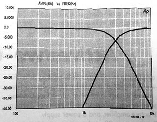
If the amplifier is used to drive the two-way loudspeaker described elsewhere in this section, the signal to the tweeter must be attenuated by about 4.5 dB.
Finally, it was noted in the prototypes that increasing the value of C9-C12 to 0.022 uF gave a rather smoother frequency response.


