Introduction
The field of electronics has seen remarkable advancements in the past few decades, leading to the development of various innovative circuits and devices. One such circuit that has gained immense popularity is the 100W 2N3055 Bridge Amplifier Circuit Diagram. This circuit is widely used in audio amplification applications and offers excellent performance characteristics.
As the name suggests, the 100W 2N3055 Bridge Amplifier Circuit employs the popular 2N3055 transistor as the main component. This transistor is known for its high power-handling capability and excellent audio amplification properties. In this article, we will explore the working principle, circuit diagram, and specifications of the 2N3055 transistor, along with two other commonly used transistors – 2N3904 and 2N3906.
Specifications of the 2N3055 Transistor
The 2N3055 transistor is an epitome of power, known for its excellent performance in audio amplifier circuits. Here are the specifications of this transistor:
- Maximum Collector-Emitter Voltage (Vce): 60V
- Maximum Collector Current (Ic): 15A
- Maximum Power Dissipation (Pd): 115W
- DC Current Gain (hfe): 20-70
- Collector-Emitter Saturation Voltage (Vce(sat)): 1.1V at Ic = 4A
The 2N3055 transistor is housed in a TO-3 package, which allows efficient heat dissipation and ensures better reliability in high-power applications. It is widely used in various audio amplifiers, power supplies, and voltage regulators.
Specifications of the 2N3904 Transistor
The 2N3904 is a general-purpose NPN transistor that finds extensive use in low-power amplification and switching applications. Here are its specifications:
- Maximum Collector-Emitter Voltage (Vce): 40V
- Maximum Collector Current (Ic): 200mA
- Maximum Power Dissipation (Pd): 625mW
- DC Current Gain (hfe): 100-300
- Collector-Emitter Saturation Voltage (Vce(sat)): 0.2V at Ic = 10mA
The 2N3904 transistor is typically housed in a TO-92 package, which makes it suitable for small, low-power circuits. It is commonly used in small audio amplifiers, signal processors, and digital circuits.
Specifications of the 2N3906 Transistor
The 2N3906 is a versatile PNP transistor that shares similarities with its NPN counterpart, the 2N3904. It is widely employed in low-power and switching applications. Here are its specifications:
- Maximum Collector-Emitter Voltage (Vce): 40V
- Maximum Collector Current (Ic): 200mA
- Maximum Power Dissipation (Pd): 625mW
- DC Current Gain (hfe): 100-300
- Collector-Emitter Saturation Voltage (Vce(sat)): 0.2V at Ic = 10mA
Similar to the 2N3904, the 2N3906 transistor
Circuit Diagram of 2N3055 Bridge Amplifier Circuit
This project can be designed using a few basic components. The circuit diagram of this project is shown below.


More Circuit Layouts


Components List of 2N3055 Bridge Amplifier Circuit
Following is the list of all components used in this project:
- 2N3055 Transistor x 4
- 2N3904 Transistor x 1
- 2N2906 Transistor x 1
- 0.33 ohms 5W Resister x 4
- 100 ohms Resister x 1
- 15 ohms Resister x 1
- 47 ohms Resister x 3
- 470 ohms Resister x 1
- 2.2k Resister x 2
- 1uF Capacitor x 1
- 4700uF Capacitor x 1
- 1N4001 Diode x 2
Working Principle of the 2N3055 Bridge Amplifier Circuit
To understand the working of the 100W 2N3055 Bridge Amplifier Circuit, let’s begin with its basic principle of operation. This circuit operates on the bridge topology, which involves the configuration of two sets of transistors in a bridge pattern. This allows for greater efficiency and power output compared to other amplifier topologies.
The input audio signal is first coupled to the base of audio transistors through a 1uf coupling capacitor. The first transistor acts as an amplifier, which enhances the weak input signal and then feeds it to the bridge arrangement of four transistors – 2N3055. These transistors drive the loudspeakers connected to the output of the circuit. The bridge configuration ensures both positive and negative half-cycles of the amplified audio signal are utilized, resulting in higher power output and improved efficiency.
Conclusion
In conclusion, the 100W 2N3055 Bridge Amplifier Circuit is an effective circuit design that utilizes 2N3055 transistors to provide a powerful output of 100 watts. The bridge configuration allows for increased efficiency and power handling capability, making it suitable for a wide range of audio applications.
The use of 2N3055 transistors ensures reliable and stable performance, with their high voltage and current handling capacities. This makes the circuit suitable for driving a variety of speakers or other audio devices with high power requirements.
Furthermore, the 2N3055 transistors can handle high temperatures, allowing for continuous operation without the risk of overheating. This guarantees a long lifespan and durability of the amplifier circuit.
Overall, the 100W 2N3055 Bridge Amplifier Circuit Diagram is a robust and efficient design that delivers high-quality audio output. It provides ample power for various audio applications and can be an excellent choice for both professional audio systems and DIY projects.
More projects, You may like:
- Video Transmitter DIY Homemade FM Radio Transmitter
- Adjustable Power Supply DIY Battery Charger
- 12V-220V 500 Watt inverter DIY Homemade
- 12V-220V H-Bridge Inverter DIY Homemade
- MPPT Solar Charge Controller DIY Homemade
- 18650 battery bank free charge protection module
- D718 B688 Bass Amplifier Homemade DIY
- C5200 Bass Amplifier DIY Homemade with Volume
- DIY LA4440 bass amplifier homemade
- C5200 A1943 TDA2030 Amplifier DIY Homemade
For more project and circuit diagrams, you can go through the Schematics in the main menu where you can find many interesting projects and circuit diagrams like audio amplifier circuits, voltage booster circuit, battery charger circuit and timer circuits etc., which are all beginner circuit projects. Feel free to check them out!
Thank you for visiting the article.
You may also like:
 100W HiFi Amplifier Circuit Diagram using 2SC3280 Transistors
- Infra-Red Proximity Detector Circuit Diagram
- Build Your Own Stereo Amplifier with TDA1552 DIY
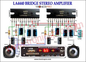
- LA4440 Bridge Stereo Amplifier Circuit Diagram
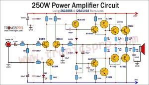
- 1000W Power Amplifier Circuit Diagram using 2SC5200 & 2SA1943 Transistors
- Unity Gain Amplifier LM1877 Circuit Diagram
- 150W HiFi Amplifier Circuit using Sanken 2SC2922 & 2SA1216
- Switch-Mode Power Supply Circuit Diagram