Introduction
If you’re interested in electronics, then the TDA2030 IC is definitely worth exploring. This small and versatile integrated circuit is a popular choice for audio amplifier designs due to its simplicity and compact size. In essence, the TDA2030 acts as a power amplifier, receiving input signals from a variety of sources (such as your phone or computer) and amplifying them to produce higher-quality sound through speakers or headphones. It operates on a low voltage, making it energy efficient as well. With some basic knowledge in electronics, it’s not too difficult to get started with the TDA2030 IC – you can even find pre-made PCBs that simplify the process of building an amplifier around this chip. Whether you’re looking to add some oomph to your home stereo system or just curious about how audio amplification works, diving into the world of TDA2030 ICs is definitely worth considering. Here are some Top TDA2030 Amplifier Circuit Diagrams provided below to start with.
List of Amplifiers TDA2030
- TDA2030 Amplifier Single Supply Circuit Diagram
- TDA2030 Amplifier Split Supply Circuit Diagram
- TDA2030 Bridge Amplifier 35W Circuit Diagram
- TDA2030 Stereo Amplifier Circuit Diagram
This chip comes with several key specifications, including an operating voltage range of 6-36V and a current output capability of up to 5A. It also boasts low distortion, -80dB PSRR (Power Supply Rejection Ratio), and high gain bandwidth products. Additionally, the TDA2030 IC can deliver an output power of up to 14W at a load impedance of 4 ohms with ±14V symmetrical power supply. Its compact size and low cost make it an ideal choice for hobbyist projects, small-scale audio amplification projects or even for constructing advanced audio systems requiring clean sound and high efficiency operation. Regardless of your audio amplifier requirements or technical prowess, you can’t go wrong with the specifications offered by this highly popular IC.
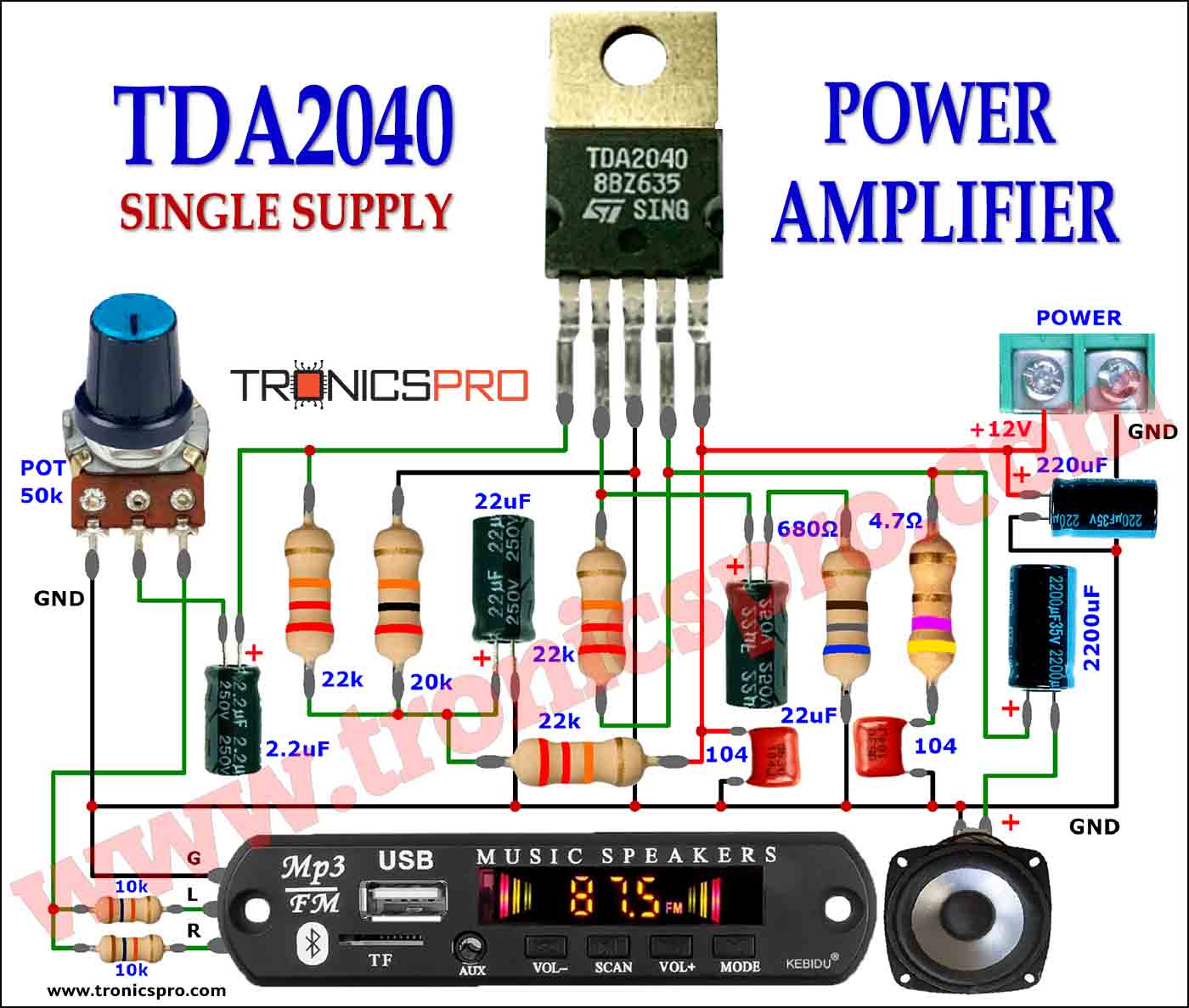
TDA2030 Amplifier Single Supply Circuit Diagram
The TDA2030 is a single supply amplifier that delivers excellent performance and can be used in various applications. This amplifier is capable of producing high-quality sound output while operating on a single voltage source. It boasts an impressive power output of up to 14 watts and features short-circuit protection, thermal shutdown, and low harmonic distortion. The TDA2030 also has a simple, easy-to-use design which makes it ideal for use by amateurs and professionals alike. Furthermore, it can accommodate input voltages ranging from -44V to +44V, which is quite impressive for a device in its class. Whether you want to use the TDA2030 for your home theatre system or vocational applications such as guitar amplifiers or PA systems, its flexibility and reliability make it one of the best options on the market today.
Circuit Diagram
of Single Supply Amplifier
More Circuit Layouts


PCB Layout of Single Supply Amplifier
TDA2030 Amplifier Split Supply Circuit Diagram
A bipolar supply configuration, also called a split supply configuration, is a type of circuit design. It involves splitting the power supply into two equal and opposite polarities. The polarities are distinguished by voltage levels, with one being positive and the other negative. The configuration is frequently utilized in audio amplifiers because it enables a signal swing that is twice the voltage level of single supply circuits. As a result, there is a boost in the amplifier’s output power and a decrease in its distortion levels.
Circuit Diagram
of Split Supply Amplifier
More Circuit Layouts


PCB Layout of Split Supply Amplifier
TDA2030 Bridge Amplifier 35W Circuit Diagram
Utilizing a sole TDA2030 IC, the TDA2030 bridge amplifier has been engineered to generate a potential output of 35 watts (at a 4 ohm load). It is an ideal choice for incorporation into audio-related devices like CD players, radios and other equipment that deals with audio streaming.
Circuit Diagram
of Bridge Amplifier
TDA2030 Stereo Amplifier Circuit Diagram
Containing only a handful of components, the Stereo Amplifier is a straightforward circuit design. It incorporates a TDA2030 IC as the primary audio amplifier, along with a few capacitors, resistors, two potentiometers, and a power supply. The TDA2030 IC is a class AB audio amplifier IC renowned for producing superior audio output with minimal distortion. With the ability to deliver up to 35W of audio output power, this IC is a versatile option for a variety of audio applications, as it operates on a split supply voltage in this circuit ranging from 9V to 24V DC.
Circuit Diagram
of Stereo Amplifier
More projects, You may like:
- Video Transmitter DIY Homemade FM Radio Transmitter
- Adjustable Power Supply DIY Battery Charger
- 12V-220V 500 Watt inverter DIY Homemade
- 12V-220V H-Bridge Inverter DIY Homemade
- MPPT Solar Charge Controller DIY Homemade
- 18650 battery bank free charge protection module
- D718 B688 Bass Amplifier Homemade DIY
- C5200 Bass Amplifier DIY Homemade with Volume
- DIY LA4440 bass amplifier homemade
- C5200 A1943 TDA2030 Amplifier DIY Homemade


