Introduction
A DC to DC converter circuit plays a crucial role in providing regulated power supply for various electronic devices, especially in situations where the input voltage needs to be stepped up or down. In this context, the utilization of a 555 Timer IC and an SL100 transistor offers a reliable and efficient solution. The 555 Timer IC, a widely used integrated circuit, serves as the core component responsible for generating and controlling the oscillations required for voltage conversion. The SL100 transistor, on the other hand, provides the necessary amplification and switching capabilities. This article explores the construction, working principle, and benefits of the DC to DC converter circuit utilizing a 555 Timer IC and an SL100 transistor.
The converter, based on the CMOS version of the 555 timer (TLC555), changes a positive potential of 9 V into a negative one of the same level and is ideal for use where a single battery is to power a circuit requiring a symmetrical supply.
DC to DC Converter Circuit Diagram
This project can be designed using a few basic components. The circuit diagram of this project is shown below.
More Circuit Layouts




Components List of DC to DC Converter Circuit
Following is the list of all components used in this project:
- IC1 … 555 IC x 1
- T1 … SL100 Transistor x 1
- C1 … 100uf Capacitor x 1
- C2 … 10uf Capacitor x 1
- C3 … 0.01uf Capacitor x 1
- R1 … 10k Resister x 1
- R2 … 470 ohms Resister x 1
- VR1 . 1M ohms Resister x 1
- D1,D2 .. 1N4001 Diodes x 2
- RL … 12V Relay x 1
- TR … 12-0-12V x 230V Transformer x 1
- BZ … 230V Buzzer x 1
Working Explanation of DC to DC Converter Circuit
If a TLC555 is not available, a Type 7555 may be used instead. The device is arranged as an astable multivibrator (AMV) with R2, R3 and C1 determining the operating frequency., which is about 20 kHz in this case.
The square wave produced by the AMV is fed to cascode rectifier C3-D1-D2-C4. Schottky diodes are better because of their lower forward voltage drop of about 0.4 V compared with 0.7 V in the case of silicon diodes and because of the higher frequency of oscillations. The rectified voltage is smoothed by C4, while C5 serves to bypass high frequency noise.
The input supply voltage to IC1 is decoupled by R1, C6 and C7. The current drawn by the converter depends largely on the load connected to the -9 V output. The output current may rise to about 10 mA before the output voltage collapses.
Conclusion of DC to DC Converter Circuit
In conclusion, the DC to DC converter circuit employing a 555 Timer IC and an SL100 transistor demonstrates exceptional efficiency and flexibility in voltage conversion. By intelligently utilizing the characteristics of these components, the circuit ensures a regulated and stable power supply, making it suitable for a diverse range of applications. Additionally, the integration of the 555 Timer IC and SL100 transistor enables effective control, amplification, and switching of the voltage, making the circuit highly reliable and efficient. Overall, this circuit offers an excellent solution for overcoming voltage fluctuations and providing a steady power supply to electronic devices, underscoring its significance in modern electronics.
More projects, You may like:
- Video Transmitter DIY Homemade FM Radio Transmitter
- Adjustable Power Supply DIY Battery Charger
- 12V-220V 500 Watt inverter DIY Homemade
- 12V-220V H-Bridge Inverter DIY Homemade
- MPPT Solar Charge Controller DIY Homemade
- 18650 battery bank free charge protection module
- D718 B688 Bass Amplifier Homemade DIY
- C5200 Bass Amplifier DIY Homemade with Volume
- DIY LA4440 bass amplifier homemade
- C5200 A1943 TDA2030 Amplifier DIY Homemade
For more project and circuit diagrams, you can go through the Schematics in the main menu where you can find many interesting projects and circuit diagrams like audio amplifier circuits, voltage booster circuit, battery charger circuit and timer circuits etc., which are all beginner circuit projects. Feel free to check them out!

Thank you for visiting the article.


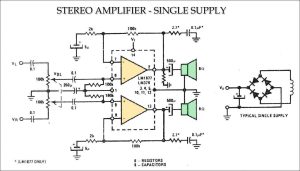


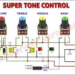


The cct diagram is not a DC-DC converter nor does it match the description.
Has the wrong diagram been posted?