Introduction
The TDA2040 is a powerful class AB amplifier integrated circuit (IC) designed for use in audio and hi-fi applications. It has a maximum output power of 30 watts and can operate from a single supply voltage of up to 45 volts. In this article, we will discuss how to build a 30W bridge amplifier using the TDA2040.
In this circuit, two TDA2040 ICs are configured in a bridge mode to deliver a high-power output. The bridge circuit configuration allows the amplifier to effectively double the voltage swing across the load, making it more efficient than a conventional single-ended amplifier.
Circuit Diagram
of 30W Bridge Amplifier TDA2040
The circuit diagram for our 30W bridge amplifier is shown below.
More Circuit Layouts
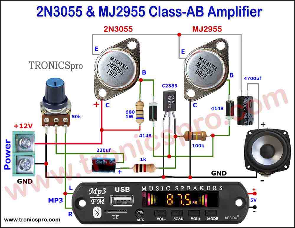

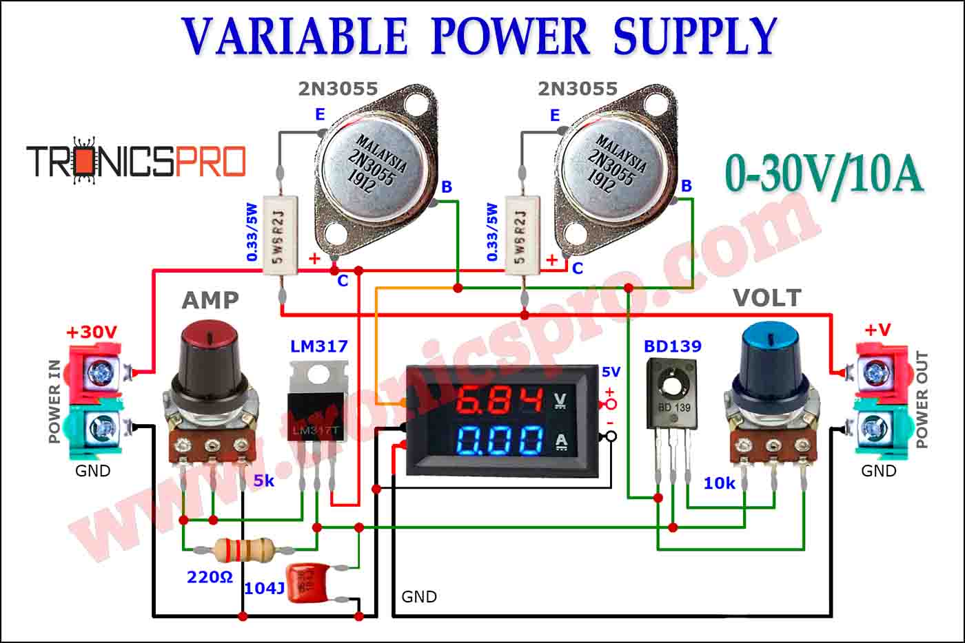


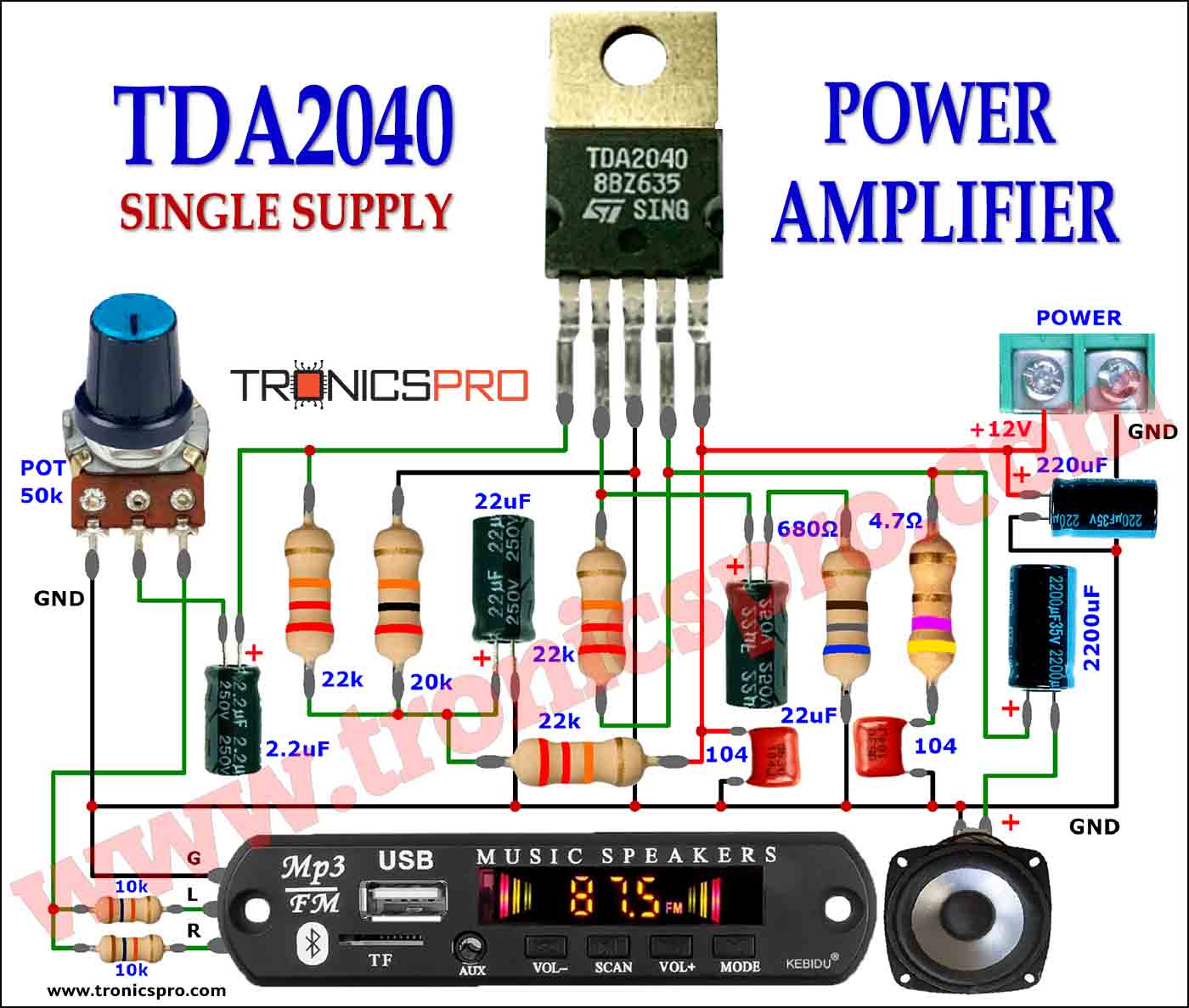

Working Explanation
of 30W Bridge Amplifier TDA2040
The input signal is fed through resistor C1 to the non-inverting input of IC1. Similarly, the inverted signal is fed to the non-inverting input of IC2. The feedback loops help to stabilize the amplifier’s gain and reduce distortion. The output from both ICs is connected in parallel to deliver a high power output. The output is filtered through the RC network consisting of R4,R6 and C4,C5, which filters out high-frequency noise and provides a stable load for the amplifier.
The power supply for the amplifier is provided by a simple rectifier circuit consisting of transformer, diodes, and smoothing capacitor. The transformer steps down the AC input voltage to a suitable level and isolates the circuit from the mains supply. The diodes rectify the AC voltage to provide a DC voltage, which is then smoothed by Capacitor to provide a stable supply voltage.
Assembling:
Once you have gathered all the required components, the circuit can be assembled on a breadboard or a printed circuit board (PCB). The following steps outline the assembly process:
- Start by soldering the components onto the PCB or breadboard, following the circuit diagram.
- Connect the input signal to the circuit through R1.
- Connect a load to the output of the amplifier.
- Connect the power supply to the circuit. Ensure that the polarity is correct.
- Adjust the gain of the amplifier using RV1.
Testing:
Once the circuit is assembled, it should be tested to ensure that it is functioning correctly. The following steps outline the testing process:
- Apply a suitable input signal to the amplifier (e.g. a sinewave).
- Measure the output voltage across the load. The voltage should not exceed the maximum rated voltage for the load.
- Measure the quiescent current of the amplifier. This should be less than 50mA.
- Measure the gain of the amplifier using an oscilloscope or multimeter. Adjust RV1 to obtain the desired gain value.
- Check the quality of the output signal for distortion and noise.
Conclusion
The 30W bridge amplifier using the TDA2040 IC is a powerful and versatile design that can be used in a wide range of audio applications. The bridge amplifier configuration allows for maximum output power with minimal distortion and noise.
More projects, You may like:
- Video Transmitter DIY Homemade FM Radio Transmitter
- Adjustable Power Supply DIY Battery Charger
- 12V-220V 500 Watt inverter DIY Homemade
- 12V-220V H-Bridge Inverter DIY Homemade
- MPPT Solar Charge Controller DIY Homemade
- 18650 battery bank free charge protection module
- D718 B688 Bass Amplifier Homemade DIY
- C5200 Bass Amplifier DIY Homemade with Volume
- DIY LA4440 bass amplifier homemade
- C5200 A1943 TDA2030 Amplifier DIY Homemade


