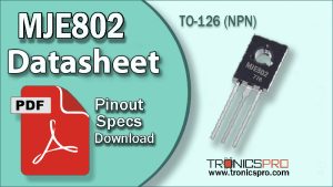
The 2N5322 transistor is a PNP silicon transistor designed for medium-power amplification and switching applications. It serves as the complementary pair of the 2N5320 NPN transistor, allowing for balanced and efficient push-pull amplifier configurations. The 2N5322 pinout follows a standard Emitter–Base–Collector (E–B–C) sequence, housed in a robust TO-39 metal can package, making it ideal for both audio and driver circuitry where stability and heat dissipation are essential.
With a collector-emitter voltage (Vce) of –75 V, a collector-base voltage (Vcb) of –100 V, and a collector current (Ic) rating of 2 A, the 2N5322 is capable of delivering up to 10 W of power dissipation while maintaining excellent frequency response and linearity.

Introduction to 2N5322 PNP Transistor
The 2N5322 PNP transistor belongs to a family of metal-can power devices widely used in amplifier drivers, audio circuits, and medium-current switching applications. It is designed to provide consistent performance under varying loads, and its complementary NPN counterpart, the 2N5320, allows designers to create symmetrical circuits with minimal distortion.
Engineers prefer the 2N5322 for its high voltage capacity, excellent gain stability, and TO-39 enclosure, which efficiently dissipates heat, ensuring reliability in continuous operation environments such as power regulators and audio amplifiers.
2N5322 PNP Transistor

Pinout of 2N5322

Pin Configuration of 2N5322 Pinout
| Pin# | Pin Name |
|---|---|
| 1 | Emitter |
| 2 | Base |
| 3 | Collector |
Key Features of 2N5322 Transistor
- General-purpose PNP silicon transistor for medium-power use
- Complementary to 2N5320 NPN transistor
- Excellent thermal conductivity via TO-39 metal case
- Suitable for driver and output amplifier stages
- High voltage tolerance and stable current gain
- Reliable performance in switching and analog circuits
2N5322 Transistor Datasheet and Specifications
- Transistor Type: PNP Silicon
- Collector-Emitter Voltage (Vce): –75 V
- Collector-Base Voltage (Vcb): –100 V
- Emitter-Base Voltage (Veb): –5 V (typical)
- Collector Current (Ic): –2 A
- Total Power Dissipation (Ptot): 10 W
- DC Current Gain (hFE): 30 – 120 (typical)
- Transition Frequency (fT): up to 50 MHz
- Junction Temperature (Tj): –65 °C to +200 °C
- Package Type: TO-39 Metal Can
- Pin Configuration: Emitter – Base – Collector (E–B–C)
Equivalent and Alternative Transistors
The 2N5322 PNP transistor can be replaced with several equivalents or substitutes that offer similar voltage, current, and package ratings:
- 2N4033 – PNP, TO-39, 80V, 1A
- BD140 – PNP, TO-126, 80V, 1.5A
- MJE15031 – PNP, TO-220, 150V, 8A
- 2N2907A – PNP, TO-18, 60V, 800mA
- 2N5415 – PNP, TO-39, 80V, 1A
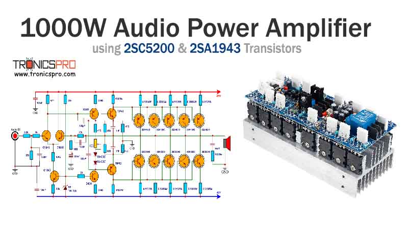
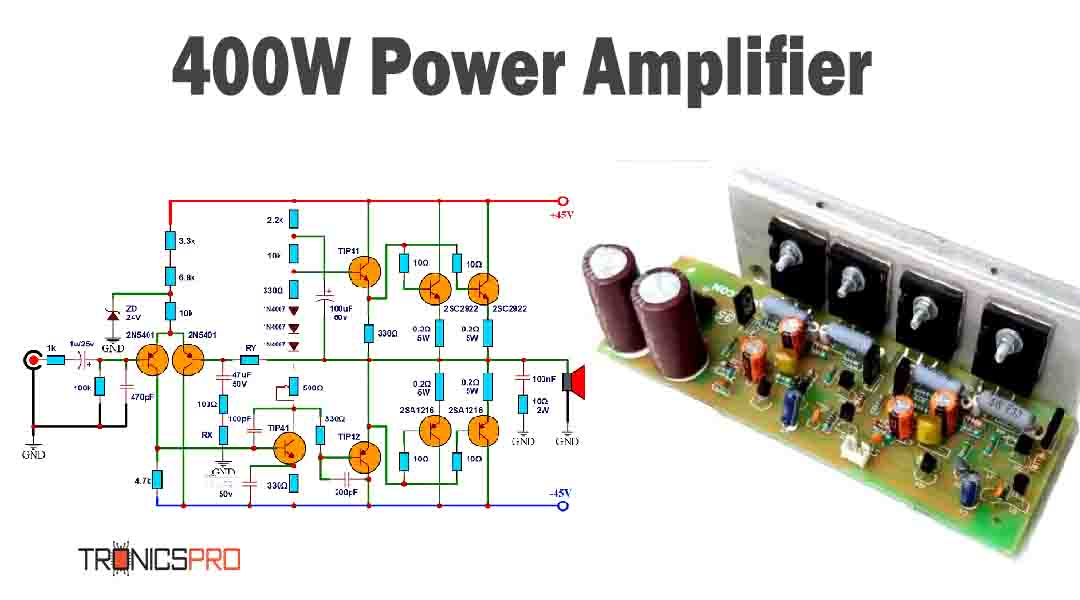
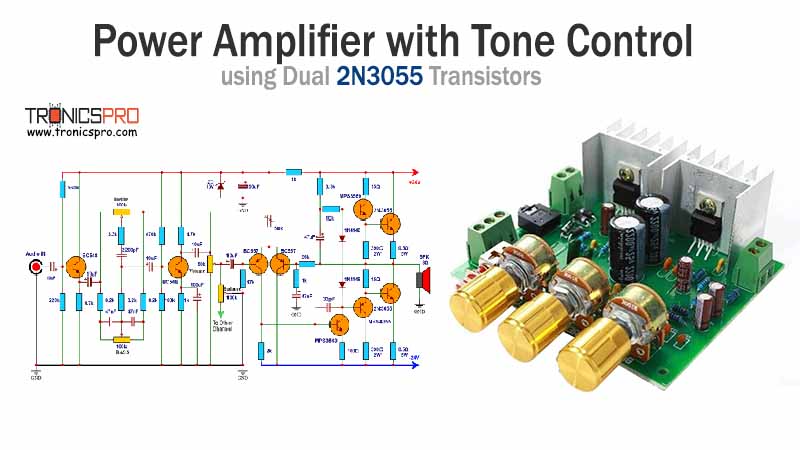
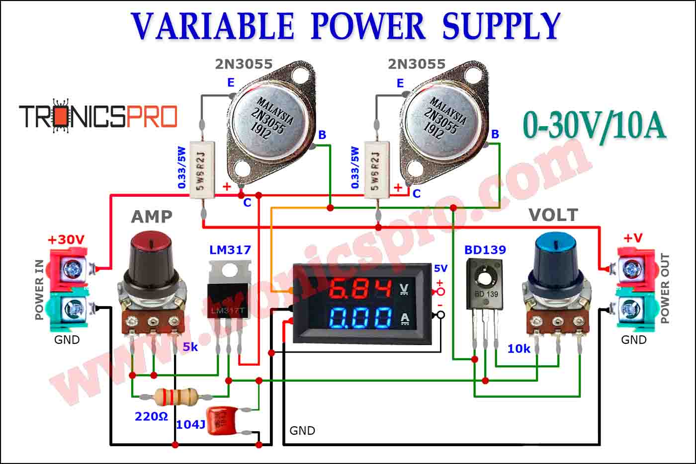
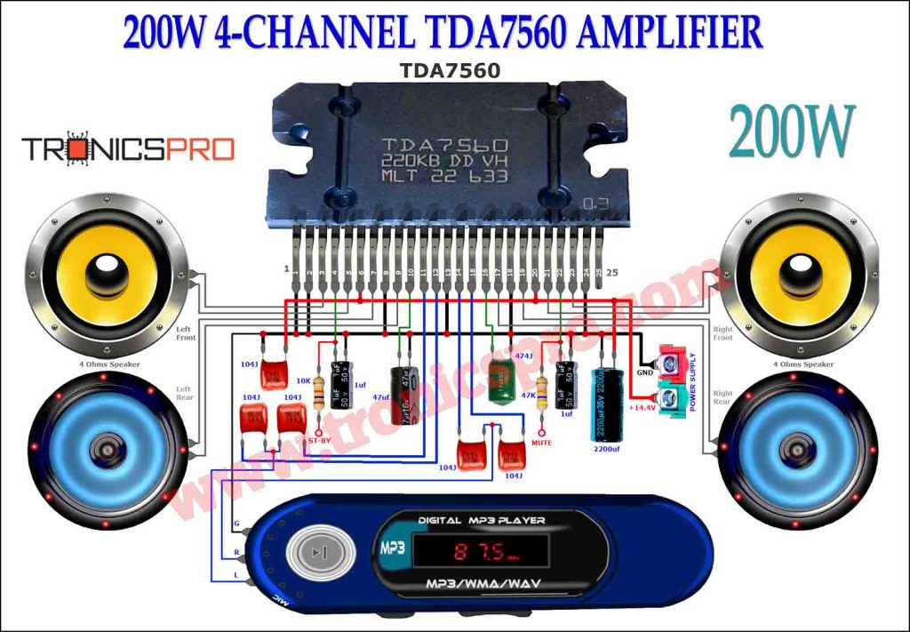
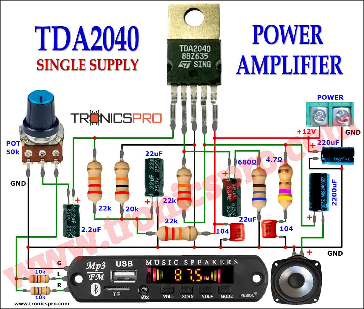
More Circuit Layouts


Applications of 2N5322 Transistor
The 2N5322 is widely used in both consumer and industrial circuits requiring medium-current amplification and signal switching. Typical uses include:
- Audio output stages and driver amplifiers
- Complementary push-pull circuits with 2N5320
- Voltage regulators and power supply controllers
- Switching regulators and low-frequency oscillators
- Relay and solenoid drivers
- Signal and pulse amplification in control systems
Its ability to handle 2 A of current and 10 W of power makes it suitable for circuits demanding moderate gain with high stability.
Working Principle of 2N5322 Transistor
The 2N5322 operates as a PNP bipolar junction transistor (BJT) where a negative base current controls the larger emitter-collector current flow. When the base is at a lower potential than the emitter, the transistor conducts, allowing current to flow from emitter to collector.
It functions in active mode for amplification, and in saturation or cutoff for switching purposes. The transistor’s balanced gain and voltage capacity make it a solid choice for both analog and pulse-driven applications.
NPN Complementary Transistor
The 2N5320 NPN transistor is the complementary device to the 2N5322 PNP transistor. Both share identical electrical parameters, differing only in polarity. Together, they are commonly used in class AB audio amplifiers, push-pull driver circuits, and output stages where linearity and symmetry are critical.
The complementary operation between 2N5320 and 2N5322 ensures equal gain response and reduced harmonic distortion, resulting in cleaner and more efficient audio amplification.
Comparison Summary: 2N5322 vs 2N5320
Although both transistors share the same structure and power ratings, their polarities define their specific circuit roles:
- The 2N5322 is a PNP transistor, meaning current flows from emitter to collector, activated by a low base potential.
- The 2N5320, on the other hand, is an NPN transistor, where current flows from collector to emitter, activated by a positive base potential.
- Used together, they form push-pull amplifier pairs, offering better efficiency, higher output power, and lower crossover distortion in audio and driver circuits.
This complementary pairing makes them ideal for designing stereo amplifiers, regulated power outputs, and high-reliability signal stages.
Advantages of 2N5322 Transistor
- High voltage tolerance up to –100V
- Medium current capacity of 2A for output stages
- Metal TO-39 package for strong thermal management
- Excellent gain linearity for low distortion in amplifiers
- Complementary pairing option with 2N5320 for push-pull design
Conclusion
The 2N5322 PNP transistor is a powerful and reliable device ideal for medium-power switching and amplification. With a –75V collector-emitter rating, 2A current capacity, and 10W power dissipation, it delivers consistent performance across audio, control, and industrial systems.
When paired with the 2N5320 NPN transistor, it forms a robust complementary pair that ensures efficiency, low distortion, and thermal reliability, making it a top choice for both analog and linear amplifier designs.
Datasheet & Pinout of 2N5322 PNP Transistor
Click the following Button to download the datasheet of 2N5322 Transistor :
More projects, You may like:
- Video Transmitter DIY Homemade FM Radio Transmitter
- Adjustable Power Supply DIY Battery Charger
- 12V-220V 500 Watt inverter DIY Homemade
- MPPT Solar Charge Controller DIY Homemade
- DIY LA4440 bass amplifier homemade
For more project and circuit diagrams, you can go through the Schematics in the main menu where you can find many interesting projects and circuit diagrams like audio amplifier circuits, voltage booster circuit, battery charger circuit and timer circuits etc., which are all beginner circuit projects. Feel free to check them out!

Thank you for visiting the article.


