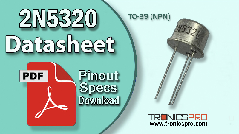
The 2N5320 transistor is a high-frequency NPN silicon transistor designed for audio, switching, and driver stage applications. It offers excellent linearity and thermal stability in a durable TO-39 metal can package, and 2N5320 pinout making it ideal for precision amplifier designs and medium-power signal circuits.
With a collector-emitter voltage (Vce) of 75 V, collector-base voltage (Vcb) of 100 V, and a collector current (Ic) rating of 2 A, the 2N5320 NPN transistor provides strong performance in medium-power amplification and regulated switching environments. The 2N5322 PNP transistor serves as its complementary pair, allowing designers to create push-pull amplifier configurations or complementary output stages.
Introduction to 2N5320 NPN Transistor
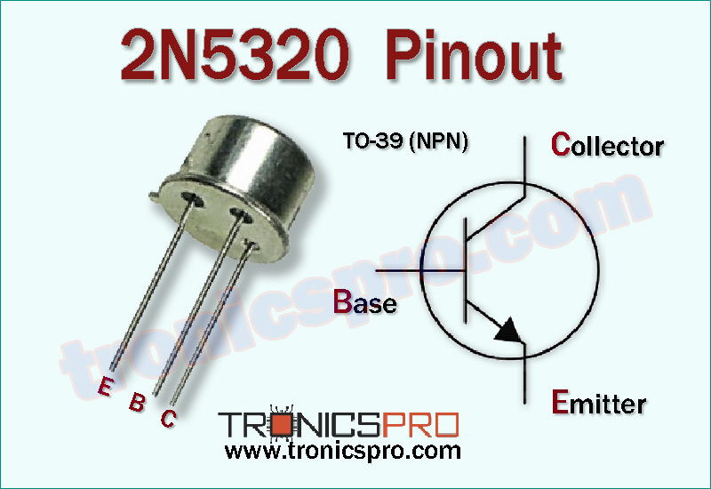
The 2N5320 belongs to the family of metal-can medium-power NPN transistors used in both analog and digital circuit designs. It features an Emitter-Base-Collector (E-B-C) pin sequence and can handle up to 10 W of total power dissipation.
This transistor is favored for audio pre-driver and driver stages, regulated power supplies, and signal amplification due to its high voltage tolerance and good frequency response. Its TO-39 metal enclosure provides superior heat conduction compared to plastic-encapsulated packages, enhancing reliability under continuous operation.
2N5320 NPN Transistor
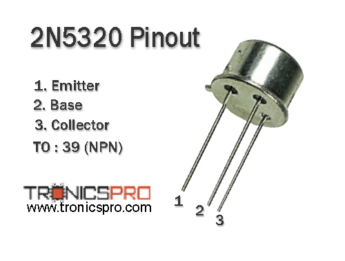
Pinout of 2N5320
Pin Configuration of 2N5320 Pinout
| Pin# | Pin Name |
|---|---|
| 1 | Emitter |
| 2 | Base |
| 3 | Collector |
Key Features of 2N5320 Transistor
- General-purpose NPN silicon transistor for medium-power circuits
- Excellent linear gain characteristics and high frequency response
- TO-39 metal can package ensures superior heat dissipation
- Stable performance over wide temperature ranges
- Suitable for audio drivers, power amplifiers, and switching stages
- Complementary transistor: 2N5322 (PNP)
2N5320 Transistor Datasheet and Specifications
- Transistor Type: NPN Silicon
- Collector-Emitter Voltage (Vce): 75 V
- Collector-Base Voltage (Vcb): 100 V
- Emitter-Base Voltage (Veb): 5 V (typical)
- Collector Current (Ic): 2 A
- Total Power Dissipation (Ptot): 10 W
- DC Current Gain (hFE): 30 – 120 (typical)
- Transition Frequency (fT): up to 50 MHz (typical)
- Junction Temperature (Tj): –65 °C to +200 °C
- Package Type: TO-39 Metal Can
- Pin Configuration: Emitter – Base – Collector (E-B-C)
Equivalent and Alternative Transistors
The 2N5320 can be replaced with other medium-power NPN transistors having similar electrical ratings and pin configuration:
- 2N3440 – 120 V, 1 A, TO-39
- 2N5550 – 140 V, 600 mA, TO-92
- MJE15030 – 150 V, 8 A, TO-220
- BD139 – 80 V, 1.5 A, TO-126
- 2N3053 – 40 V, 700 mA, TO-39
More Circuit Layouts


Applications of 2N5320 Transistor
The 2N5320 NPN transistor is commonly used in medium-power amplification and driver designs, including:
- Audio amplifier driver stages
- Power supply regulator circuits
- Signal amplifiers in instrumentation systems
- Relay and solenoid drivers
- Switching regulators and oscillator circuits
- Complementary amplifier pairs with 2N5322
Its robust TO-39 design allows it to operate effectively in high-reliability or industrial applications that require moderate power and voltage tolerance.
Working Principle of 2N5320 Transistor
The 2N5320 functions as a bipolar junction transistor (BJT) in which a small base current controls a larger collector current. When a positive voltage is applied to the base relative to the emitter, it allows current to flow from collector to emitter.
Operating in active mode, it acts as a linear amplifier, while in saturation and cutoff, it behaves as a digital switch. The combination of high voltage capacity and controlled current gain makes it efficient for both modes of operation.
PNP Complementary Transistor
The 2N5322 is the PNP complementary transistor to the 2N5320. Both share similar voltage, current, and power ratings, enabling their use in complementary push-pull output stages or class-AB amplifier circuits.
The 2N5322 conducts when the base is driven low, while the 2N5320 conducts when the base is driven high, forming a balanced pair ideal for audio output stages, inverter circuits, and driver amplifiers that require symmetrical performance.
Comparison Summary: 2N5320 vs 2N5322
Both transistors share the same structural design and electrical characteristics, differing only in polarity:
- The 2N5320 is an NPN transistor, while the 2N5322 is its PNP complement.
- The 2N5320 allows current to flow from collector to emitter when the base is forward-biased, whereas the 2N5322 allows flow in the reverse direction when the base is pulled negative.
- Together, they are often paired in push-pull or complementary amplifier stages, delivering higher efficiency and lower distortion in power audio circuits.
This complementary relationship makes the pair particularly useful in stereo amplifier designs and output driver systems.
Advantages of 2N5320 Transistor
- Metal can (TO-39) design provides excellent thermal stability
- High voltage tolerance up to 100 V collector-base
- Wide current range up to 2 A for medium-power applications
- Compatible with complementary transistor (2N5322) for push-pull use
- Good frequency response for low to mid-frequency circuits
Conclusion
The 2N5320 NPN transistor is a durable and versatile medium-power device ideal for both amplification and switching operations. With 75 V collector-emitter voltage, 2 A current handling, and 10 W power dissipation, it bridges the gap between small-signal and high-power transistors.
Its E-B-C pin configuration, metal TO-39 package, and complementary PNP partner (2N5322) make it an excellent choice for designers seeking reliability, thermal efficiency, and balanced circuit performance in industrial, audio, and analog applications.
Datasheet & Pinout of 2N5320 NPN Transistor
Click the following Button to download the datasheet of 2N5320 Transistor :
More projects, You may like:
- Video Transmitter DIY Homemade FM Radio Transmitter
- Adjustable Power Supply DIY Battery Charger
- 12V-220V 500 Watt inverter DIY Homemade
- MPPT Solar Charge Controller DIY Homemade
- DIY LA4440 bass amplifier homemade
For more project and circuit diagrams, you can go through the Schematics in the main menu where you can find many interesting projects and circuit diagrams like audio amplifier circuits, voltage booster circuit, battery charger circuit and timer circuits etc., which are all beginner circuit projects. Feel free to check them out!
Thank you for visiting the article.
You may also like:
![2N3055 NPN Transistor]()
2N3055 NPN Transistor - Datasheet
![MJL21193 PNP Transistor Datasheet]()
MJL21193 PNP Power Transistor Datasheet
![bd907 datasheet pinout]()
BD907 Pinout, Equivalent, Applications, Datasheet
![bd545 datasheet pinout]()
BD545 Pinout, Equivalent, Applications, Datasheet
![2n6098 datasheet pinout equivalent specification]()
2N6098 Pinout, Equivalent, Application, Datasheet
![bd649 datasheet pinout]()
BD649 Pinout, Equivalent, Applications, Datasheet
![2SD718 NPN Transistor Datasheet Pinout]()
2SD718 NPN Transistor Datasheet & Pinout
![bf421 datasheet pinout equivalent specification application transistor]()
BF421 Pinout, Equivalent, Application, Datasheet