The 2N2369 pinout represents a high-speed NPN transistor designed for fast switching and pulse applications. This transistor is widely used in digital logic circuits, oscillators, and RF amplifiers where speed and precision are essential.
Encased in a TO-18 metal can package, the 2N2369 offers low capacitance, fast rise and fall times, and stable operation at high frequencies, making it a preferred choice in both analog and digital electronic designs.

Introduction to 2N2369 NPN Transistor
The 2N2369 is a silicon planar epitaxial NPN bipolar junction transistor (BJT) optimized for high-speed switching and amplification. It is capable of operating with up to 15V collector-emitter voltage (Vce) and 70V collector-base voltage (Vcb), while handling a collector current (Ic) up to 200mA.
This transistor’s high transition frequency and short storage time make it ideal for high-speed digital switching, pulse shaping, and timing circuits. It is frequently used in logic gates, RF drivers, and oscillator networks requiring rapid transitions and minimal delay.
2N2369 NPN Transistor
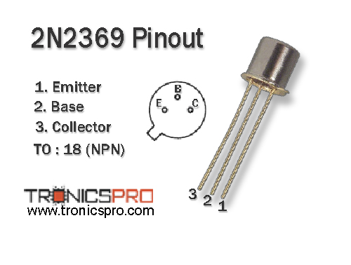
Pinout of 2N2369

Pin Configuration of 2N2369 Pinout
| Pin# | Pin Name |
|---|---|
| 1 | Emitter |
| 2 | Base |
| 3 | Collector |
Understanding the 2N2369 Pinout Configuration
The 2N2369 pinout follows the Emitter–Base–Collector (E–B–C) sequence when viewed from the bottom side of its TO-18 metal can package (leads downward). This layout simplifies prototyping and allows easy substitution with other small-signal NPN transistors having the same pin configuration.
Key Features of 2N2369 Transistor
- High-speed NPN transistor for fast switching applications
- Compact TO-18 metal package with excellent heat dissipation
- Low saturation voltage for efficient signal control
- Short storage time for clean, sharp transitions
- High transition frequency suitable for RF and digital circuits
- Reliable performance in logic, timing, and pulse circuits
2N2369 Transistor Datasheet and Specifications
- Collector-Emitter Voltage (Vce): 15 V
- Collector-Base Voltage (Vcb): 70 V
- Emitter-Base Voltage (Veb): 5 V
- Collector Current (Ic): 200 mA
- Total Power Dissipation (Ptot): 360 mW
- DC Current Gain (hFE): 40 – 120
- Transition Frequency (fT): 500 MHz typical
- Storage Time: <10 ns
- Package Type: TO-18 Metal Can
- Pinout Configuration: Emitter–Base–Collector (E–B–C)
- Polarity Type: NPN
- Junction Temperature (Tj max): 200 °C
Equivalent and Alternative Transistors
The 2N2369 equivalent transistors include:
Always verify the pin configuration and maximum ratings before substitution to ensure proper circuit operation.
More Circuit Layouts


Applications of 2N2369 Transistor
- High-speed digital switching circuits
- RF amplifiers and signal boosters
- Oscillator and waveform generation circuits
- Logic-level pulse shaping and timing
- Frequency multipliers and drivers
- Fast logic inverters and test pulse generators
Working Principle of 2N2369 Transistor
The 2N2369 transistor operates by using a small current applied to its base terminal to control a larger current flow between collector and emitter. In switching mode, it quickly transitions between ON and OFF states, making it ideal for digital circuits and pulse generation.
Its high transition frequency (around 500 MHz) and low storage time allow it to operate effectively in radio frequency (RF) and ultra-fast logic circuits, maintaining stable performance under varying conditions.
In amplification mode, the transistor boosts input signals with minimal distortion, suitable for high-frequency small-signal amplifiers.
Frequently Asked Questions (FAQ)
What is the 2N2369 transistor used for?
It is mainly used in high-speed switching, digital pulse, and RF circuits due to its rapid response and low storage time.
What is the 2N2369 pinout?
The 2N2369 pinout follows the Emitter–Base–Collector (E–B–C) configuration when viewed from the bottom of the TO-18 package.
Is 2N2369 suitable for RF applications?
Yes, it offers a transition frequency up to 500 MHz, making it suitable for RF amplifiers, oscillators, and signal modulation circuits.
What is the difference between 2N2369 and 2N2369A?
The 2N2369A is an enhanced version of the 2N2369 with improved switching speed and reduced storage time.
How much current can the 2N2369 handle?
It can handle a maximum collector current of 200 mA, making it suitable for low to moderate current switching tasks.
Conclusion
The 2N2369 NPN transistor is a compact, high-speed device widely used in logic, pulse, and RF applications. Its fast switching performance, low power dissipation, and reliable metal TO-18 package make it a go-to component for engineers designing high-frequency circuits and digital logic systems.
With its proven speed and consistency, the 2N2369 remains a preferred choice for precision timing and high-speed electronic applications.
Datasheet & Pinout of 2N2369 NPN Transistor
Click the following Button to download the datasheet of 2N2369 Transistor :
More projects, You may like:
- Video Transmitter DIY Homemade FM Radio Transmitter
- Adjustable Power Supply DIY Battery Charger
- 12V-220V 500 Watt inverter DIY Homemade
- MPPT Solar Charge Controller DIY Homemade
- DIY LA4440 bass amplifier homemade
For more project and circuit diagrams, you can go through the Schematics in the main menu where you can find many interesting projects and circuit diagrams like audio amplifier circuits, voltage booster circuit, battery charger circuit and timer circuits etc., which are all beginner circuit projects. Feel free to check them out!
Thank you for visiting the article.
You may also like:
![BC308 PNP Transistor Datasheet]()
BC308 PNP Transistor Pinout Datasheet
![MJE15032 NPN Transistor Pinout Datasheet]()
MJE15032 NPN Power Transistor Datasheet
![TIP3055 NPN Transistor Pinout Datasheet]()
TIP3055 NPN Transistor Pinout Datasheet
![2n5550 datasheet pinout]()
2N5550 Pinout, Equivalent, Application, Datasheet
![tip102 datasheet pinout equivalent specification application mosfet n-channel]()
TIP102 Pinout, Equivalent, Application, Datasheet
![2n5416 datasheet pinout]()
2N5416 Pinout, Equivalent, Application, Datasheet
![MJE13009 Power Transistor Datasheet]()
MJE13009 NPN Power Transistor Datasheet
![mje15031 datasheet pinout]()
MJE15031 Pinout Equivalent Application Datasheet