Introduction
An ultra-low-noise preamplifier is a powerful tool for any recording studio or live performance venue. It provides a clean, clear signal boost, reducing unwanted noise and enhancing the overall sound quality. The design of ultra low-noise preamps gives you more control over your sound, with an increased dynamic range compared to regular preamps. This means that quieter sounds and higher volumes can be achieved with minimal distortion and interference. Due to their advanced design and components, they also provide an excellent signal-to-noise ratio ensuring that unwanted ambient noise stays at a minimum. With some models also offering additional features such as line outputs and impedance switching, ultra low-noise preamps offer unprecedented versatility for your audio setup.
Circuit Diagram
of Ultra Low-Noise Preamplifier Circuit

More Circuit Layouts


Working Explanation
of Ultra Low-Noise Preamplifier Circuit
The preamplifier is intended for use with low-impedance signal sources like moving-coil pick-up cartridges used in high-end record players. The input impedance of the preamplifier is 100 ohms. To keep the input noise as low as possible, Connect three dual transistors type SSM2220 or MATO3 transistors in parallel to form a discrete differential amplifier. By connecting this amplifier ahead of IC1‚, the input noise of the op amp becomes im-material. The base connections of the discrete amplifier then function as the inputs of a super op amp with a very low input noise level. The p-n-p transistors used to score over their n-p-n counterparts in their much lower low-frequency noise level. A fairly large bias current of about 5.5 mA is created at the input. This is the result of the 2 mA setting of each transistor in combination with the relatively low gain of the p-n-p devices.
Preset P1‚ and resistors R7-R8 enable any tolerances of R4 and R5 in the differential amplifier output to be compensated. Transistor T4 and light-emitting diode D1‚ensure a stable current setting for the differential amplifier. The LED should be a flat, red, type fitted securely to T4 for thermal coupling. Because the input noise level amounts to 0.4 nV/VHz (theoretical value for a 10 ohms resistor), it is essential that the feedback adds as little as possible to the overall noise figure. Consequently, the impedance of the feedback circuit must be much lower than 10 ohms.

Furthermore, the OP27 demands a certain minimum load impedance, so that the feedback impedance may not be less than 600 ohms. To ensure that a low value can be used for R9, a compromise is necessary between maximum gain (here, approx. 24 dB or x15.7) on the one hand and the value of R9. This resistor adds 0.3 nV/VHz to the input noise level, which, based on measurement data, amounts to 0.52 nV/VHz. If more gain is needed, a noise figure of about 0.4 nV/VHz may be achieved if the value of R9 is lowered. Resistor, R1‚ ahead of the actual feedback, ensures that the opam is not excessively loaded. The obvious disadvantage of adding R11 is a higher internal gain, which causes smaller bandwidth and a lower drive margin. Fortunately, these factors are of little consequence in the case of moving-coil elements.
There are two ways of adjusting P1. The first is to adjust the output voltage to nil (measure at IC1‚ pin 6). The second is to measure the input offset, for example, 0.55 mV across 100 ohms. Assuming that the offset caused by T1‚, T2, and T3 is negligible, the output voltage of 15.68 x 0.55 mV (8.62 mV with respect to ground), measured at junction R10-R11-R12, is well balanced.
Readers may like to try the effects of reducing the number of input transistors from three to just one to reduce the input bias current. Must change the value of the resistor to 249 ohms. Bear in mind, however, that the input noise level then rises by 2.5 dB.
Capacitor C2‚ prevents any offset voltage from being applied to the input of the following amplifier.
Power the preamplifier with the symmetrical regulated 15-V supply, and draw about 16 mA from each rail.
Components List
of Ultra Low-Noise Preamplifier Circuit
- Resistors:
- R1, R12 = 100 ohms
- R2 = 15 k
- R3 = 82 ohms
- R4, R5 = 1.50 k
- R6 = 150 ohms
- R7, R8 = 39 ohms
- R9 = 5.62 ohms
- R10 = 82.5 ohms
- R11 = 511 ohms
- R13 = 100 k
- P1‚ = 50 ohms, preset, horizontal
Capacitors: - C1‚ = 0.01 uF
- C2 = 10 µF, metalized polyester (MKT), pitch
- 22.5 mm or 27.5 mm
- C3, C5, C7= 220 uF, 25 V, radial
- C4, C6 = 0.1 uF
Semiconductors: - D1 = red LED, flat
- T1, T2, T3 = SSM2220 or MAT03 (Analog Devices)
- T4 = BC560C
Integrated circuits: - IC 1 = OP27GP (Analog Devices)
Miscellaneous: - K1, K2 = phono socket, gold-plated, for PCB mounting
- Make the PCB with the aid of the track layout.
An Ultra Low-Noise Preamplifier is an invaluable piece of equipment for anyone wanting to achieve the highest quality audio available. It's designed to boost the signal from low-level sources such as record turntables, tape decks, microphones, or DACs without introducing any noise into the signal chain. The preamp works by amplifying the input voltage without overdriving it, allowing for maximum information retrieval and clean audio reproduction. As it does this, noise levels are kept extremely low which results in clear and lifelike sound with a wide dynamic range. This makes ultra low-noise preamps perfect for true audiophiles looking to experience their music at its best.
You may also like:
 120W MOSFET Amplifier Circuit Diagram using IRFP240 & IRFP9240
- Non-Inverting AC Power Amplifier Circuit Diagram
- 100W Amplifier Circuit Diagram using TIP142 & TIP147 Transistors
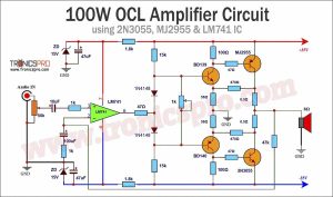
- 100W OCL Amplifier Circuit Diagram using 2N3055 & LM741 IC
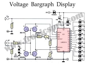
- Voltage Bargraph Display Circuit Diagram
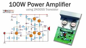
- 100W Power Amplifier Circuit Diagram using dual 2N3055 Transistor
- 3200V Power Supply Circuit Diagram
- Subwoofer Amplifier Circuit Diagram using TDA2030