Introduction
The BD434 is a silicon epitaxial-base PNP medium-power transistor engineered for linear amplification and switching applications. It belongs to a complementary pairing family, designed to work alongside NPN devices like BD433 in push-pull and audio output stages. Its PNP polarity enables it to handle negative-half cycles or high-side switching in amplifier circuits.
This transistor is housed in a TO-126 (SOT-32 / JEDEC SOT-32) plastic package, offering moderate thermal dissipation when mounted on a heatsink or circuit board. Its construction delivers good balance among gain, saturation voltage, and robustness, making it suitable for moderate-power circuits.
BD434 PNP Transistor
In practice, BD434 is widely used in audio amplifier output stages, complementary driver circuits, and general power switching roles where symmetrical PNP conduction is needed. Because it complements BD433 (its NPN counterpart), it ensures symmetrical performance in push-pull layouts, helping to reduce distortion and balance output.
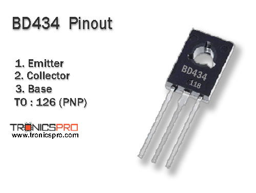
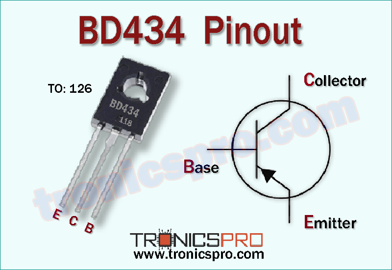
Pinout of BD434
Key Features
- PNP polarity for negative conduction / high-side switching
- Matched for complementary pairing with NPN devices
- Reliable performance in moderate-power amplifier / driver circuits
- Plastic package suitable for moderate heatsinking
- Good thermal and mechanical stability
- Widely used in audio and push-pull applications
Specifications/Characteristics
- Collector-Base Breakdown Voltage, VCBO = –22 V
- Collector-Emitter Breakdown Voltage, VCEO = –22 V
- Collector-Emitter Sustaining Voltage, VCE(sus) = –22 V
- Emitter-Base Breakdown Voltage, VEBO = –5 V
- Collector Current, Continuous IC = –4 A
- Collector Peak (Pulse) Current, ICM = –7 A
- Total Power Dissipation, Ptot = 36 W (case temperature = 25 °C)
- Maximum Junction Temperature, Tj = 150 °C
- Storage Temperature Range, Tstg = –65 to +150 °C
- DC Current Gain, hFE = 85 (at IC = 0.5 A)
- DC Current Gain, hFE = 40 (at IC = 10 mA)
- DC Current Gain, hFE = 50 (at IC = 2 A)
- Collector-Emitter Saturation Voltage, VCE(sat) = –0.58 V (IC = –2 A, IB = –0.2 A)
- Base-Emitter On Voltage, VBE(on) ≈ –1.1 to –1.2 V
- Transition Frequency, fT = 3 MHz
Pin Configuration
| Pin# | Pin Name | Pin Description |
|---|---|---|
| 1 | Emitter | Output / current source terminal |
| 2 | Collector | Main current sink terminal |
| 3 | Base | Control / bias input terminal |
Comparison of BD434 (PNP) vs BD433 (NPN) Complementary
- BD434 is a PNP transistor intended to complement BD433 (NPN), used in symmetrical amplifier or driver circuits. It conducts for negative polarity or high-side segments in push-pull operations.
- BD433, on the other hand, is the NPN side of the pair. It conducts positive cycles or lower-side segments in complementary stages.
- Because they are designed as complements, BD434 and BD433 share similar current, gain, power, and thermal characteristics (with reversed polarities), allowing them to operate together symmetrically in push-pull or class-AB amplifier designs.
More Circuit Layouts


Key Applications of BD434 PNP Transistor
- Push-pull amplifier output stages
- Audio amplifier driver circuits
- Complementary driver / output stage designs
- Switching / power regulation circuits requiring PNP conduction
- General-purpose PNP transistor applications in medium-power systems
NPN Complimentary Transistor
- The complementary NPN transistor for BD434 is BD433.
Equivalent Transistors of BD434 PNP Transistor
Possible equivalents or substitution options for BD434 include:
- BD436 (higher voltage PNP in same series)
- BD438 (even higher-voltage PNP sibling)
- Other PNP medium-power transistors such as TIP32C, MJE2955, or devices with matching current/voltage specs
- PNP power transistors in TO-126 / TO-220 packages with similar ratings
Datasheet of BD434 PNP Transistor
Click the following Button to download the datasheet of BD434 Transistor :
More projects, You may like:
- Video Transmitter DIY Homemade FM Radio Transmitter
- Adjustable Power Supply DIY Battery Charger
- 12V-220V 500 Watt inverter DIY Homemade
- MPPT Solar Charge Controller DIY Homemade
- DIY LA4440 bass amplifier homemade
For more project and circuit diagrams, you can go through the Schematics in the main menu where you can find many interesting projects and circuit diagrams like audio amplifier circuits, voltage booster circuit, battery charger circuit and timer circuits etc., which are all beginner circuit projects. Feel free to check them out!
Thank you for visiting the articl
You may also like:
![2n6288 datasheet pinout equivalent specification]()
2N6288 Pinout, Equivalent, Application, Datasheet
![mje13005 datasheet pinout equivalent specification application npn transistor]()
MJE13005 Pinout, Equivalent Application Datasheet
![TIP2955 PNP Transistor Pinout Datasheet]()
TIP2955 PNP Transistor Pinout Datasheet
![2n6476 datasheet pinout equivalent specification]()
2N6476 Pinout, Equivalent, Application, Datasheet
![2n5089 datasheet pinout]()
2N5089 Pinout, Equivalent, Application, Datasheet
![TIP35 NPN Transistor Datasheet Pinout]()
TIP35 NPN Transistor Pinout Datasheet
![2n5550 datasheet pinout]()
2N5550 Pinout, Equivalent, Application, Datasheet
![2n2905 datasheet pinout]()
2N2905 Pinout, Equivalent, Application, Datasheet