Introduction
The BD241 (and its variants BD241A/B/C) is a silicon epitaxial-base NPN power transistor designed for medium power amplifier and switching applications. It is packaged in a TO-220 plastic package, which allows effective mounting and heat dissipation in many power circuits. It is part of a complementary transistor family pairing with PNP devices like BD242.

Because the BD241 series offers multiple variants (A, B, C) with different voltage ratings (e.g. 60 V, 80 V, 100 V) it provides flexibility for designers to choose the version matching the supply voltage in their circuits. In amplifier or switching circuits, BD241 is often used in driver stages, power amplifier outputs, or as an intermediate power transistor.
BD241 NPN Transistor

The transistor is widely used in general purpose electronics because of its balance between voltage capability, current handling, and power dissipation. When matched with its complementary PNP (BD242), it enables push-pull amplifier stages and symmetrical output stages. Its “Base-Island” layout helps maintain good gain and low saturation voltage under load.
Pinout of BD241

Key Features
- Multiple voltage variants (A, B, C) for flexible design margin
- Low saturation voltage under load
- Good DC current gain stability
- TO-220 package suitable for heatsinking
- Compatible for complementary pairing with PNP devices
- Suitable for both switching and linear amplifier roles
Specifications/Characteristics
- Collector-Emitter Voltage, VCEO varies by variant (e.g. 60 V, 80 V, 100 V)
- Collector-Base Voltage, VCER (with base resistor) also variant dependent (e.g. up to 115 V for some versions)
- Emitter-Base Breakdown Voltage, VEBO = 5 V
- Continuous Collector Current, IC = 3 A
- Peak (Pulsed) Collector Current, ICM = 5 A
- Base Current, IB = 1 A (absolute max)
- Total Power Dissipation (at case temperature 25 °C), Ptot = 40 W
- Maximum Junction Temperature, Tj = 150 °C
- Storage Temperature Range, Tstg = –65 to +150 °C
- Collector-Emitter Saturation Voltage, VCE(sat) = 1.2 V (IC = 3 A, IB = 0.6 A)
- Base-Emitter On Voltage, VBE(on) = 1.8 V (IC = 3 A, VCE = 4 V)
- DC Current Gain, hFE(min) = 25 at IC = 1 A, VCE = 4 V
- DC Current Gain, hFE(min) = 10 at IC = 3 A, VCE = 4 V
- Thermal Resistance, Junction-to-Case, θJC = 3.12 °C/W
- Thermal Resistance, Junction-to-Ambient, θJA = 62.5 °C/W
Pin Configuration
| Pin# | Pin Name | Pin Description |
|---|---|---|
| 1 | Base | Signal / drive input terminal |
| 2 | Collector | Main current output terminal |
| 3 | Emitter | Return / ground side terminal |
Comparison BD239 vs BD241 vs BD243
- BD239 is a member of the same transistor family but often with somewhat lower voltage ratings (for example 100 V collector-emitter) and designed for amplifier and switching roles in moderate voltage designs. Its structure favors general-purpose use.
- BD241 typically offers higher voltage variants (60 V, 80 V, 100 V) which gives it more headroom in circuits with higher supply voltages, while maintaining strong current capability and power dissipation. It is a more versatile choice when the design might see voltage stress.
- BD243 is the higher-voltage side of this transistor family, engineered to handle more extreme voltage conditions (often with higher collector-emitter and collector-base voltage specs). It is suited for circuits with large supply voltages or where robustness against voltage transients is required.
- All three BD239, BD241, and BD243 are built to deliver similar continuous current in the mid-ampere range and are often used in amplifier or switching roles. The key difference lies in their maximum voltage tolerances (how much stress they can endure), so designers choose between them based on the voltage environment their circuit will face, while relying on similar current and power handling and switching/gain behavior.
More Circuit Layouts

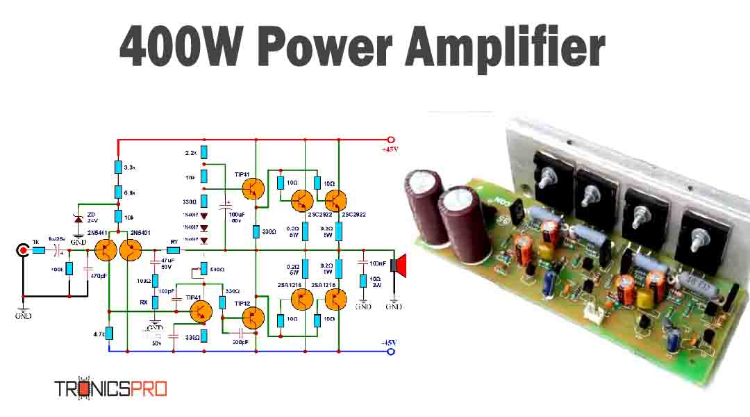
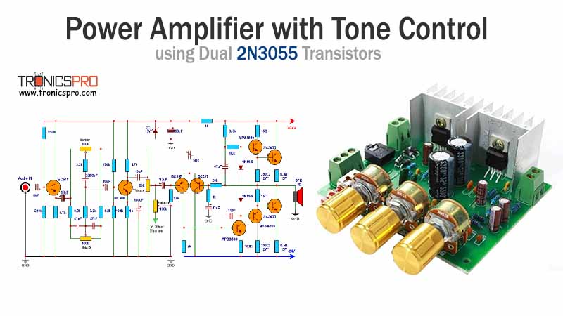
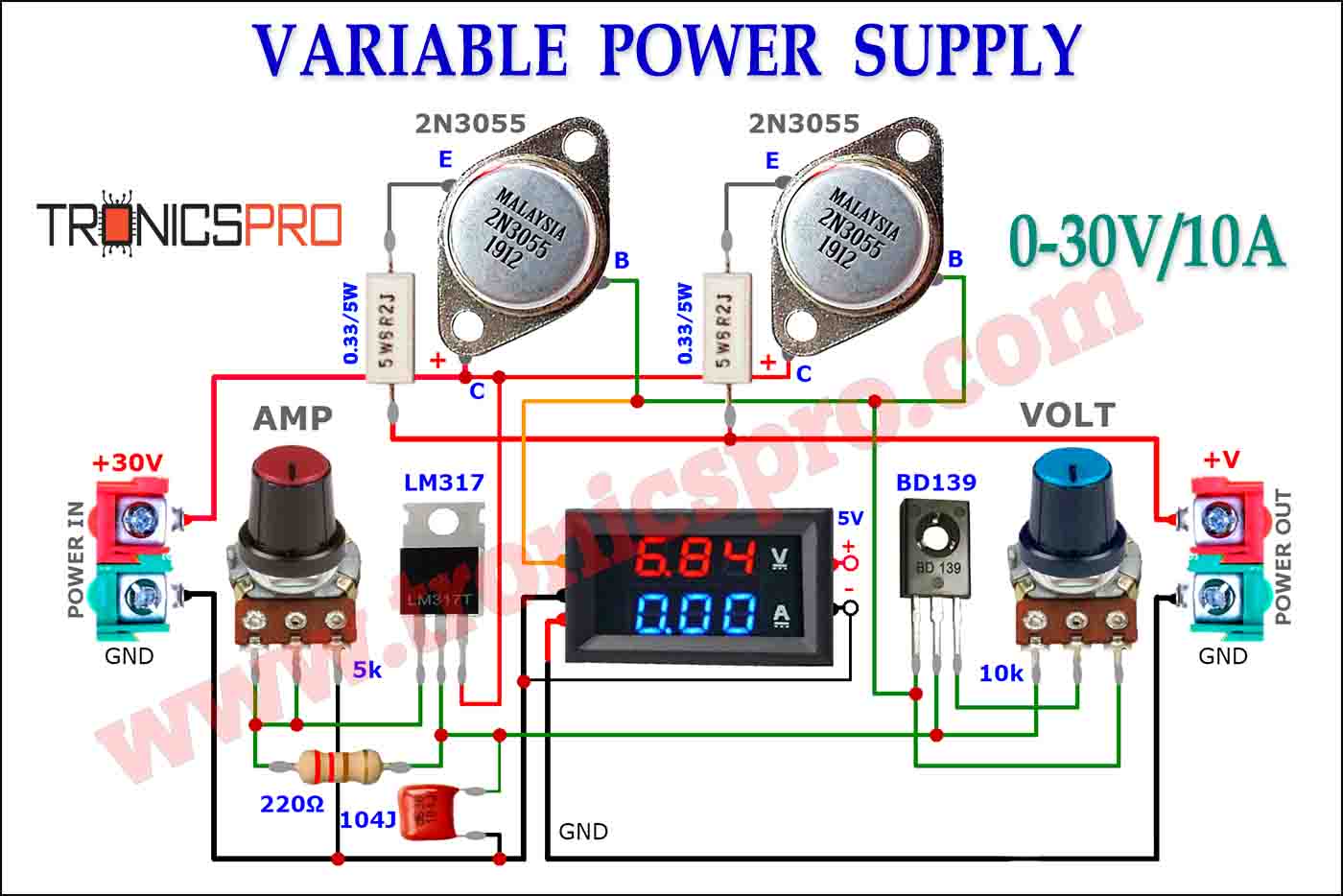

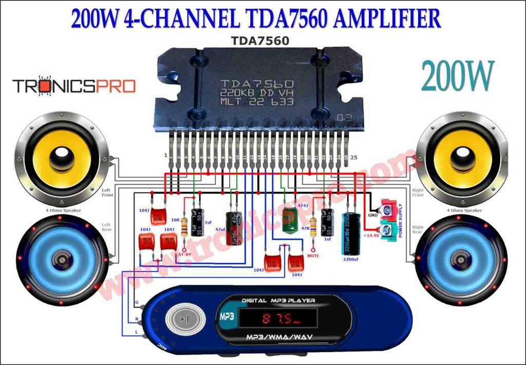
Key Applications of BD241 NPN Transistor
- Push-pull amplifier output stages
- Audio amplifier drivers
- General switching circuits in power supplies
- Signal interfacing and buffer stages
- Medium-power linear and switching applications
PNP Complimentary Transistor
- The PNP complementary counterpart to BD241 (for each variant) is BD242 (i.e. BD242A, BD242B, BD242C)
Equivalent Transistors of BD241 NPN Transistor
Some possible equivalents or alternatives for BD241 include:
- Other NPN transistors in similar voltage/current class (e.g. TIP31, MJL series)
- Different variants within BD241 family (BD241A, BD241B, BD241C)
- NPN power transistors in TO-220 form with matching voltage/current and gain
(Pin configuration of some transistors mentioned here may different from BD241).
Datasheet of BD241 NPN Transistor
Click the following Button to download the datasheet of BD241 Transistor :
More projects, You may like:
- Video Transmitter DIY Homemade FM Radio Transmitter
- Adjustable Power Supply DIY Battery Charger
- 12V-220V 500 Watt inverter DIY Homemade
- MPPT Solar Charge Controller DIY Homemade
- DIY LA4440 bass amplifier homemade
For more project and circuit diagrams, you can go through the Schematics in the main menu where you can find many interesting projects and circuit diagrams like audio amplifier circuits, voltage booster circuit, battery charger circuit and timer circuits etc., which are all beginner circuit projects. Feel free to check them out!

Thank you for visiting the article.


