Introduction
The BD235 is a medium-power NPN silicon epitaxial-base transistor tailored for both linear amplification and switching applications. It belongs to the BD23x transistor family (BD233, BD235, BD237) and is packaged in the TO-126 (SOT-32 / Jedec SOT-32) plastic package. It is designed for reliable operation in audio driver stages, power amplifiers, and general-purpose switching circuits.

Engineered with a “Base Island” layout in planar technology, the BD235 exhibits high gain performance and low saturation voltage, making it suitable for efficient analog and switching designs. Its ratings place it between the lower-voltage BD233 and higher-voltage BD237, offering a balanced option for circuits with moderate voltage demands.
BD235 NPN Transistor

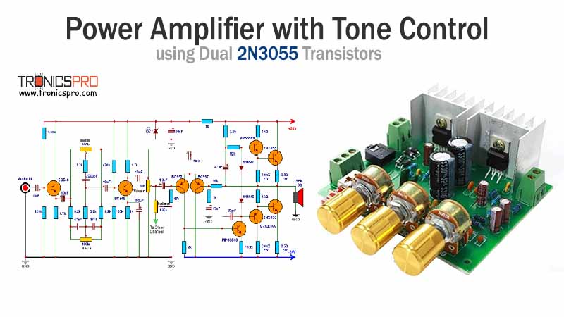
In real-world use, designers value the BD235 for its robustness in audio amplifiers, push-pull stages, and driver circuits. Because of its moderate stresses and clear datasheet parameters, it integrates well in hobbyist and industrial designs, provided temperature management and biasing are handled correctly.
Pinout of BD235

Key Features
- Balanced voltage and current capability for medium-power designs
- Low saturation voltage for efficient switching
- High current gain stability across operating range
- Package designed for easy mounting and moderate heat dissipation
- Suitable for complementary pair configurations
- Reliable for both analog and switching circuits
Specifications/Characteristics
- Collector-Base Breakdown Voltage, VCBO = 60 V
- Collector-Emitter Breakdown Voltage, VCEO = 60 V
- Collector-Emitter Voltage (R = 1 kΩ between base/emitter), VCE(RBE = 1 kΩ) = 60 V
- Emitter-Base Breakdown Voltage, VEBO = 5 V
- Collector Current (Continuous), IC = 2 A
- Collector Peak Current (Pulse), ICM = 6 A
- Collector Power Dissipation, Ptot = 25 W (Tc = 25 °C)
- Maximum Junction Temperature, Tj = 150 °C
- Storage Temperature Range, Tstg = –65 to +150 °C
- Thermal Resistance, Junction-to-Case, Rθjc = 5 °C/W
- Collector Cut-off Current (ICBO) = up to ≈ 0.1 mA (at VCE = rated)
- Emitter Cut-off Current (IEBO) = up to ≈ 1 mA (at VEB = 5 V)
- Collector-Emitter Sustaining Voltage (VCE(sus)) = 60 V (IC = 100 mA)
- Collector-Emitter Saturation Voltage, VCE(sat) = 0.6 V (IC = 1 A, IB = 0.1 A)
- Base-Emitter On Voltage, VBE(on) = 1.3 V (IC = 1 A, VCE = 2 V)
- DC Current Gain (hFE) = 40 (IC = 150 mA, VCE = 2 V)
- DC Current Gain (hFE) = 25 (IC = 1 A, VCE = 2 V)
- Transition Frequency, fT = 3 MHz (IC = 250 mA, VCE = 10 V)
Pin Configuration
| Pin# | Pin Name | Pin Description |
|---|---|---|
| 1 | Emitter | Current return / output terminal |
| 2 | Collector | Main current input terminal |
| 3 | Base | Control / drive terminal |
Comparison BD233 vs BD235 vs BD237 NPN Transistors
- The BD233, BD235, and BD237 are part of the same transistor family, sharing similar construction, gain characteristics, and package style, but each is tailored to a different voltage class. The BD233 is the lowest-voltage device, rated for 45 V collector-emitter, making it ideal for low to medium voltage amplifier and driver circuits.
- The BD235 steps up to 60 V, offering better headroom and flexibility for circuits running higher supply voltages, while still preserving the performance traits of the family.
- The BD237 offers the highest voltage acceptance, with a 80 V (or in some sources up to 100 V) rating on collector-emitter, making it suitable for more demanding or higher-voltage switching and amplification tasks.
- In terms of current capability, all three transistors support the same continuous collector current of 2 A and a peak pulse current of 6 A, which means they are interchangeable from a current-handling standpoint but differ in what maximum voltages they can safely endure. Their power dissipation ratings are also consistent (25 W), indicating the same thermal constraints in design. Because they share the same package and general architecture, the key differentiator in selecting among them is the supply or signal voltage level.
- Use BD233 for lower-voltage designs, BD235 for intermediate levels, and BD237 when extra voltage margin is needed—while maintaining uniformity in gain, saturation voltage, and switching behavior.
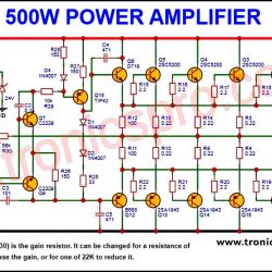
More Circuit Layouts


Key Applications of BD235 NPN Transistor
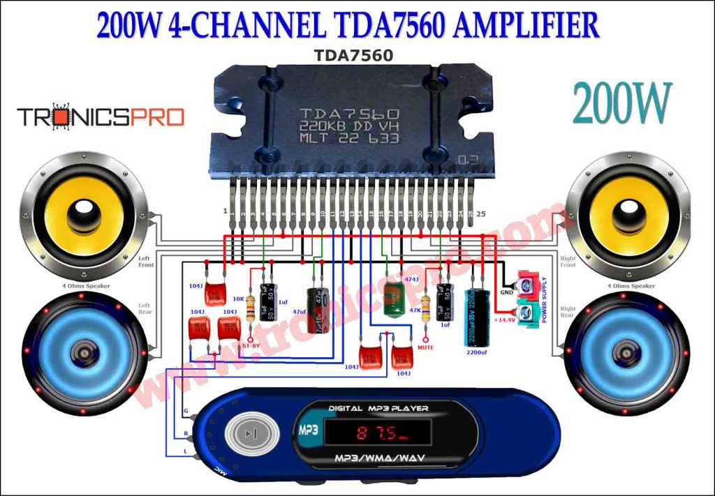
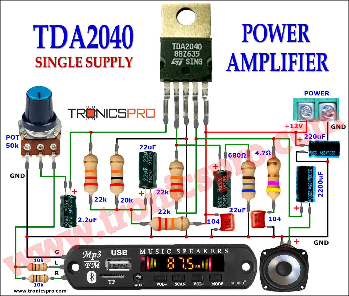
- Audio amplifier driver stages
- Push-pull complementary amplifier circuits
- Medium power switching circuits (relays, motors)
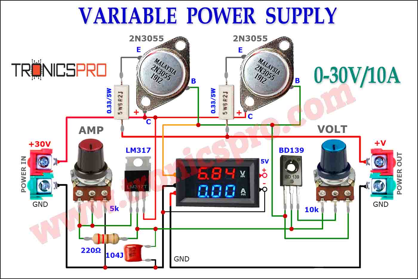
- Linear power supplies and voltage regulators
- Signal amplification in general-purpose electronics
PNP Complimentary Transistor
- The PNP complementary transistor of BD235 is BD236
Equivalent Transistors of BD235 NPN Transistor
Some possible alternatives or equivalents to BD235 include:
- BD233 (in lower voltage applications)
- BD237 (in higher voltage applications)
- TIP41 (for somewhat higher current or power designs)
- 2N3055 (for heavier duty power applications)
(Pin configuration of some transistors mentioned here may different from BD235).
Datasheet of BD235 NPN Transistor
Click the following Button below to download the datasheet of BD235Transistor :
More projects, You may like:
- Video Transmitter DIY Homemade FM Radio Transmitter
- Adjustable Power Supply DIY Battery Charger
- 12V-220V 500 Watt inverter DIY Homemade
- MPPT Solar Charge Controller DIY Homemade
- DIY LA4440 bass amplifier homemade
For more project and circuit diagrams, you can go through the Schematics in the main menu where you can find many interesting projects and circuit diagrams like audio amplifier circuits, voltage booster circuit, battery charger circuit and timer circuits etc., which are all beginner circuit projects. Feel free to check them out!

Thank you for visiting the article.


