The 2N5415 is a silicon PNP bipolar junction transistor (BJT) designed for high-voltage, medium-power switching and amplification. It features a TO-39 metal can package that ensures excellent thermal performance and rugged durability. The 2N5415 pinout follows the Emitter-Base–Collector (E–B-C) configuration, making it suitable for use in analog driver circuits, power regulators, and general amplifier stages requiring high voltage tolerance.
With a collector-emitter voltage (Vce) of –200 V, collector-base voltage (Vcb) of –200 V, and a collector current (Ic) of –1 A, this transistor provides a power dissipation of 10 W. These features make it ideal for use in circuits that demand high breakdown strength and reliable switching at elevated voltages.

Introduction to 2N5415 PNP Transistor
The 2N5415 belongs to a family of high-voltage PNP transistors commonly used in audio, RF, and industrial control applications. Because of its high breakdown voltage and robust structure, it performs exceptionally well in push-pull amplifiers, linear regulators, and switching circuits.
Its metal-can TO-39 package offers good heat dissipation, allowing stable operation even under continuous load. This makes the 2N5415 an excellent choice for medium-power driver stages, signal amplification, and power control systems that must handle high voltage without distortion.
2N5415 PNP Transistor

Pinout of 2N5415

Pin Configuration of 2N5415 Pinout
| Pin# | Pin Name |
|---|---|
| 1 | Emitter |
| 2 | Base |
| 3 | Collector |
Key Features of 2N5415 Transistor
- Silicon PNP transistor for high-voltage operation
- TO-39 metal case ensures excellent heat transfer
- High breakdown voltage up to 200 V
- Stable DC current gain and low noise performance
- Ideal for amplification and medium-power switching
- Reliable thermal stability and long service life
2N5415 Transistor Datasheet and Specifications
- Transistor Type: PNP Silicon
- Collector-Emitter Voltage (Vce): –200 V
- Collector-Base Voltage (Vcb): –200 V
- Emitter-Base Voltage (Veb): –5 V (typical)
- Collector Current (Ic): –1 A
- Power Dissipation (Ptot): 10 W
- DC Current Gain (hFE): 20 – 100 (typical range)
- Transition Frequency (fT): 50 MHz (typical)
- Junction Temperature (Tj): –65 °C to +200 °C
- Package Type: TO-39 Metal Can
- Pin Configuration: Base – Collector – Emitter (B–C–E)
Equivalent and Alternative Transistors
The 2N5415 transistor can be replaced with the following PNP high-voltage equivalents that share similar performance:
- 2N5416 – PNP, TO-39, –250 V, –1 A
- BD140 – PNP, TO-126, –80 V, –1.5 A
- MJE350 – PNP, TO-126, –300 V, –0.5 A
- 2N4037 – PNP, TO-39, –150 V, –800 mA
- 2N2905A – PNP, TO-39, –60 V, –800 mA
Ensure that voltage and current ratings match the circuit requirements when selecting a substitute.
More Circuit Layouts



Applications of 2N5415 Transistor
The 2N5415 is widely used in high-voltage control and amplification systems, including:
- Audio amplifier driver stages
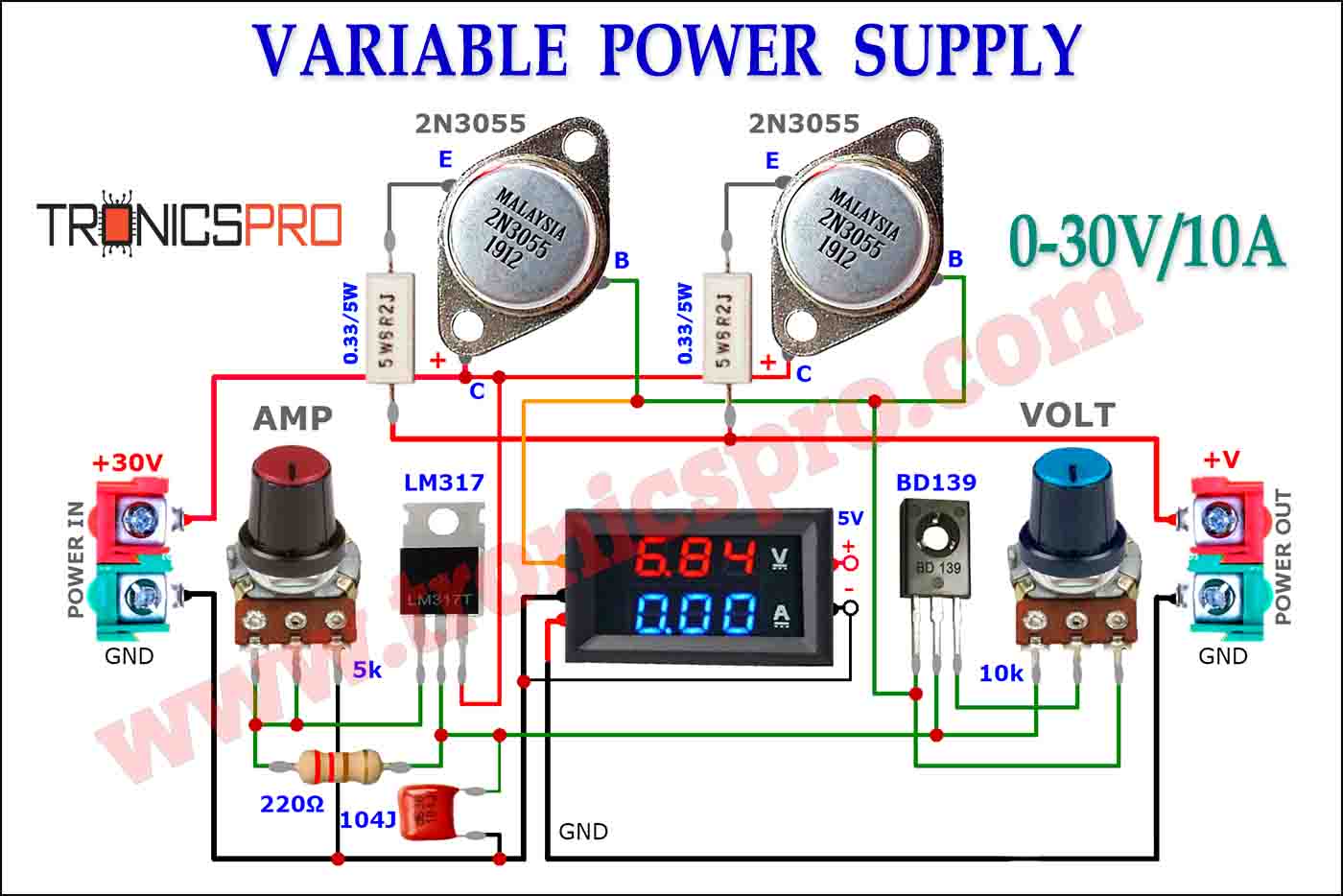
- Voltage regulation and power supply circuits
- High-voltage switching applications
- Industrial automation systems
- Analog signal processing
- Power inverters and feedback control modules
Its stable characteristics make it a dependable option for both analog and digital interface circuits.
Working Principle of 2N5415 Transistor
In the 2N5415 PNP transistor, current flows from the emitter to the collector when a small reverse bias current is applied to the base–emitter junction. The transistor remains ON when the base is at a lower potential than the emitter.
In amplification mode, it operates within the active region, amplifying input signals with high linearity. In switching mode, it functions as a fast and efficient electronic switch, suitable for power control and driver modules in high-voltage environments.
Advantages of 2N5415 Transistor
- Supports up to –200 V operation
- Excellent thermal stability due to TO-39 metal design
- Low leakage current and high gain consistency
- Compatible with medium-power circuits
- Long-term reliability in industrial environments
Conclusion
The 2N5415 PNP transistor is a versatile and durable device built for high-voltage applications in audio, power, and industrial circuits. With a voltage capacity of –200 V, a collector current of –1 A, and 10 W power dissipation, it ensures reliable performance across a range of uses.
Its E–B-C pin layout, metal TO-39 package, and stable electrical characteristics make it a preferred choice for engineers designing medium-power amplifiers, voltage regulators, and signal driver circuits.
Datasheet & Pinout of 2N5415 PNP Transistor
Click the following Button to download the datasheet of 2N5415 Transistor :
More projects, You may like:
- Video Transmitter DIY Homemade FM Radio Transmitter
- Adjustable Power Supply DIY Battery Charger
- 12V-220V 500 Watt inverter DIY Homemade
- MPPT Solar Charge Controller DIY Homemade
- DIY LA4440 bass amplifier homemade
For more project and circuit diagrams, you can go through the Schematics in the main menu where you can find many interesting projects and circuit diagrams like audio amplifier circuits, voltage booster circuit, battery charger circuit and timer circuits etc., which are all beginner circuit projects. Feel free to check them out!

Thank you for visiting the article.


