Introduction
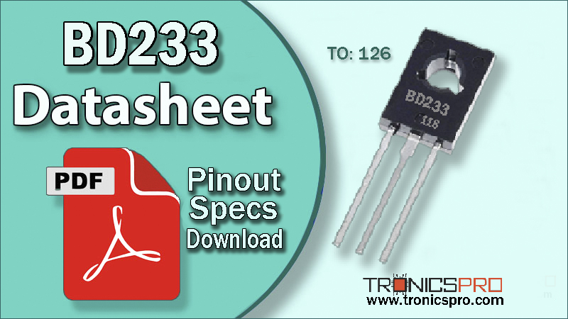
The BD233 is a medium-power NPN silicon transistor designed for linear and switching applications. It is often used in audio amplifier stages, driver circuits, and general purpose power switching tasks thanks to its balance of moderate voltage and current handling. The BD233 is designed in a TO-126 plastic package, which offers compactness and reasonable thermal performance when mounted on a heatsink or circuit board.
Because of its moderate breakdown voltages and reasonable gain, BD233 is well suited for applications where you don’t need ultra-high voltage but require stability and reliability in medium power domains. Its features support both linear amplification (audio, pre-drivers) and switching (relay drivers, power regulation). It is commonly paired with its PNP complement, enabling push-pull or complementary amplifier designs.
BD233 NPN Transistor

In practical circuits, the BD233 provides stable performance up to its limits, but care must be taken in thermal design and biasing to avoid saturation losses and thermal runaway. The transistor’s parameters such as gain, saturation voltage, and switching times are well documented, letting designers reliably integrate it into amplifier stages or switching modules with predictable results.
Pinout of BD233

Key Features
- Medium power transistor suitable for both switching and linear use
- Complementary pairing capability (for push-pull designs)
- Moderate transition frequency enabling reasonable bandwidth
- Compact TO-126 package for ease of mounting
- Good thermal stability under rated conditions
- Balanced trade-off of voltage, current, and gain for general use
Specifications/Characteristics
- Collector-Base Breakdown Voltage, VCBO = 45 V
- Collector-Emitter Breakdown Voltage, VCEO = 45 V
- Collector-Emitter Sustaining Voltage, VCE(sus) = 45 V (IC = 100 mA, IB = 0)
- Emitter-Base Breakdown Voltage, VEBO = 5 V
- Collector Current, Continuous IC = 2 A
- Collector Current, Peak (Pulse) ICM = 6 A
- Base Current, continuous IB = 0.5 A
- Collector Power Dissipation, PC = 25 W (at TC = 25 °C)
- Junction Temperature, Tj = 150 °C
- Storage Temperature Range, Tstg = –65 to +150 °C
- Collector Cut-off Current, ICBO = up to ~100 µA (VCB = 45 V, IE = 0)
- Emitter Cut-off Current, IEBO = up to ~1 mA (VEB = 5 V, IC = 0)
- DC Current Gain, hFE (min) = 40 (IC = 150 mA, VCE = 2 V)
- DC Current Gain, hFE (min) = 25 (IC = 1 A, VCE = 2 V)
- Collector-Emitter Saturation Voltage, VCE(sat) = 0.6 V (IC = 1 A, IB = 0.1 A)
- Base-Emitter On Voltage, VBE(on) = 1.3 V (IC = 1 A, VCE = 2 V)
- Transition Frequency, fT = 3 MHz (IC = 250 mA, VCE = 10 V)
- Turn-On Time, tON ≈ 0.4 to 1.0 µs
- Turn-Off Time, tOFF ≈ 1.5 to 3.0 µs
Pin Configuration
| Pin# | Pin Name | Pin Description |
|---|---|---|
| 1 | Emitter | Output / current return terminal |
| 2 | Collector | Main current input terminal |
| 3 | Base | Control terminal (input) |
Comparison (BD233 vs BD235 vs BD237) NPN Transistors
- The BD233, BD235, and BD237 are all NPN silicon medium-power transistors designed in the TO-126 package, belonging to the same transistor family series. They share similar mechanical characteristics and current-handling capabilities but differ mainly in their voltage ratings, which define the operating limits and suitable applications for each device.
- The BD233 is the lowest-voltage variant in the family, with a typical collector-emitter voltage (VCEO) rating of 45 V. It is best suited for low to medium voltage amplifier circuits and switching applications where supply voltages are modest, typically up to 24 V systems. Because of its lower voltage rating, the BD233 has slightly higher gain consistency at lower voltages and can operate more efficiently within that range.
- The BD235 increases the collector-emitter voltage rating to 60 V, offering improved tolerance against higher voltage spikes and transients. This makes it more suitable for circuits powered by 30 V or higher rails, such as driver stages or industrial control systems. The current gain and frequency characteristics remain similar to BD233, but BD235 provides greater safety margin in voltage-sensitive designs.
- The BD237 is the highest-voltage version of the three, with a collector-emitter voltage (VCEO) of 80 V. It is intended for higher voltage switching and amplifier stages where more headroom is needed, such as in automotive, motor-driver, or regulated power supplies. While the BD237’s gain (hFE) is typically similar to that of BD233 and BD235, its higher voltage structure results in slightly higher saturation voltage and a marginally slower switching response at maximum rated current.
- In terms of collector current, all three transistors share the same rating of 2 A continuous and 6 A peak, ensuring identical load-driving capability. Their power dissipation ratings are also equivalent, around 25 W at 25 °C case temperature, given identical TO-126 packaging. The transition frequency (fT) across the family is about 3 MHz, which means all three are suitable for low-frequency to moderate-speed switching applications.
- Overall, BD233 is ideal for low-voltage amplifier and driver circuits, BD235 serves as a balanced middle option for moderate voltage designs, and BD237 provides the highest voltage tolerance for demanding or industrial environments. Designers often select among them purely based on the maximum voltage requirement while keeping other parameters consistent, as the three are electrically and mechanically interchangeable within their rated limits.
More Circuit Layouts


Key Applications of BD233 NPN Transistor
- Audio amplifier stages and drivers
- Push-pull complementary amplifier circuits
- General switching circuits (relays, motors)
- Linear regulation and driver circuits
- Medium power signal amplification
PNP Complimentary Transistor
- The BD233’s complementary PNP transistor is the BD234
Comparison BD233 vs BD234 PNP complement
- The BD233 is an NPN transistor while BD234 is its PNP complementary counterpart. In circuit use they work together in push-pull or complementary amplifier stages, with BD233 handling the positive half-cycle and BD234 handling the negative.
- The NPN BD233 conducts when its base is driven positive relative to its emitter, whereas the PNP BD234 conducts when its base is driven negative relative to its emitter. Their voltage and current ratings are intended to be matched to maintain symmetry in amplifier outputs.
- Although both share many similar electrical characteristics (gain, saturation voltage, package) their doping and internal structure differ to support opposite polarity operation. In system design, biasing and thermal matching become crucial since differences in saturation or leakage between BD233 and BD234 can lead to distortion or imbalance in output.
Equivalent Transistors of BD233 NPN Transistor
Some possible alternatives or equivalents (similar specifications) include:
- BD235 (same family, higher voltage)
- BD237 (same family, higher voltage)
- TIP41 / TIP42 (in broader class)
- 2N3055 (in larger power class)
- MJE3055 / MJE3055T (depending on voltage/current needs)
(Pin configuration of some transistors mentioned here may different from BD233).
Datasheet of BD233 NPN Transistor
Click the following Button below to download the datasheet of BD233 Transistor :
More projects, You may like:
- Video Transmitter DIY Homemade FM Radio Transmitter
- Adjustable Power Supply DIY Battery Charger
- 12V-220V 500 Watt inverter DIY Homemade
- MPPT Solar Charge Controller DIY Homemade
- DIY LA4440 bass amplifier homemade
For more project and circuit diagrams, you can go through the Schematics in the main menu where you can find many interesting projects and circuit diagrams like audio amplifier circuits, voltage booster circuit, battery charger circuit and timer circuits etc., which are all beginner circuit projects. Feel free to check them out!
Thank you for visiting the article.
You may also like:
![2n6517 datasheet pinout equivalent specification]()
2N6517 Pinout, Equivalent, Application, Datasheet
![mps2222 datasheet pinout equivalent specification]()
MPS2222 Pinout, Equivalent Application, Datasheet
![BC639 NPN Transistor Datasheet]()
BC639 NPN Transistor Pinout Datasheet
![mje15028 datasheet pinout]()
MJE15028 Pinout Equivalent Application Datasheet
![2n4427 datasheet pinout]()
2N4427 Pinout, Equivalent, Application, Datasheet
![2n4125 datasheet pinout]()
2N4125 Pinout, Equivalent, Application, Datasheet
![2n2219 datasheet pinout]()
2N2219 Pinout, Equivalent, Application, Datasheet
![BD442 PNP Transistor Datasheet]()
BD442 PNP Transistor Pinout Datasheet