

The BD115 is an NPN high-voltage transistor designed for reliable amplification and switching in demanding electronic circuits. This article explains the BD115 pinout, key features, electrical specifications, working principle, applications, and equivalent alternatives to help you use it correctly in practical designs.

Introduction
The BD115 is a high-voltage NPN bipolar junction transistor optimized for medium-power applications. With its ability to handle high collector-emitter voltages and moderate current levels, it is commonly used in amplifier stages, power control circuits, and industrial electronics requiring stable and fast transistor response.
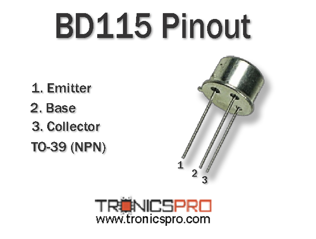
Pin Configuration / Pinout of BD115 Transistor
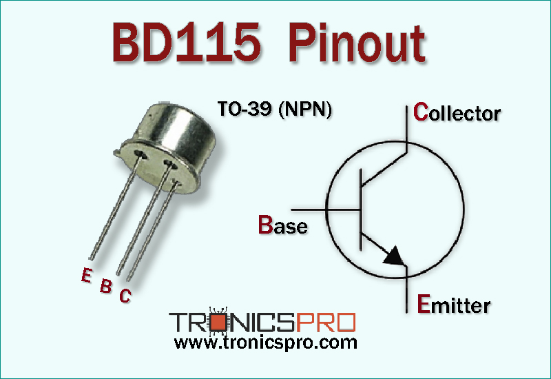
Understanding the BD115 Pinout Configuration
The BD115 comes in a TO-39 metal package and follows the E-B-C pin configuration:
| Pin# | Pin Name |
|---|---|
| 1 | Emitter |
| 2 | Base |
| 3 | Collector |
Correct understanding of the BD115 pinout is essential to ensure proper biasing, safe operation, and maximum performance.
Note: DATASHEET DOWNLOAD button is provided end of this article.
BD115 Key Features
- NPN high-voltage bipolar transistor
- Suitable for medium-power amplification
- High transition frequency for fast signal response
- Robust TO-39 metal package
- Stable gain over a wide operating range
- Designed for high-reliability electronic circuits
BD115 Specifications/Characteristics
- Collector-Emitter Voltage (Vceo): 180V
- Collector-Base Voltage (Vcbo): 245V
- Emitter-Base Voltage (Vebo): 5V
- Collector Current (Ic): 150mA
- Peak Collector Current (Icm): 200mA
- Total Power Dissipation (Ptot): 6W
- Junction Temperature (Tj): 200°C
- Storage Temperature (Tstg): −55°C to 200°C
- DC Current Gain (hFE): 60
- Transition Frequency (fT): 145MHz
Key Applications of BD115 Transistor
- High-voltage amplifier stages
- Industrial control electronics
- Power supply driver circuits
- Signal amplification in audio equipment
- Switching circuits requiring fast response
BD115 Equivalent / Alternatives
(Verify pin compatibility before using substitutions)
Equivalent Transistors:
- BD135 (voltage-rated variants may differ)
Alternative Transistors:
- BF459
- BF469
- MJE340
More Circuit Layouts


Working Principle of BD115
The BD115 operates as a current-controlled NPN transistor. When a small base current is applied between the base and emitter, it allows a larger current to flow from the collector to the emitter. This amplification mechanism enables the BD115 to function effectively in voltage amplification and switching applications, especially where high voltage handling is required.
Frequently Asked Questions (FAQ)
Q1: What type of transistor is BD115?
BD115 is an NPN high-voltage bipolar junction transistor.
Q2: What package is used by BD115?
It is available in a TO-39 metal package.
Q3: What is the BD115 pin configuration?
The BD115 follows an E-B-C pinout.
Q4: Can BD115 be used in audio amplifier circuits?
Yes, it is suitable for high-voltage audio and signal amplification stages.
Conclusion
The BD115 NPN high-voltage transistor offers a strong combination of high voltage capability, fast switching speed, and reliable thermal performance. Its TO-39 package and stable electrical characteristics make it a dependable choice for amplification and control applications in both industrial and audio electronics.
Datasheet of BD115 Transistor
Click the following Button below to download the datasheet of BD115 :
More projects, You may like:
- Video Transmitter DIY Homemade FM Radio Transmitter
- Adjustable Power Supply DIY Battery Charger
- 12V-220V 500 Watt inverter DIY Homemade
- MPPT Solar Charge Controller DIY Homemade
- DIY LA4440 bass amplifier homemade
For more project and circuit diagrams, you can go through the Schematics in the main menu where you can find many interesting projects and circuit diagrams like audio amplifier circuits, voltage booster circuit, battery charger circuit and timer circuits etc., which are all beginner circuit projects. Feel free to check them out!