The 2N5305 pinout refers to a low-power NPN transistor widely used in signal amplification and low-current switching circuits. Built in the TO-92 plastic package, this transistor provides reliable performance for hobby, educational, and commercial electronic designs. With voltage ratings of 25V (Vce) and 25V (Vcb), the 2N5305 NPN transistor offers a maximum collector current of 300mA and 400mW power dissipation, making it ideal for general-purpose low-power amplifier and driver applications.

Introduction to 2N5305 NPN Transistor
The 2N5305 transistor is a silicon-based NPN bipolar junction transistor (BJT) designed for low-current amplification and fast switching response. Because of its compact TO-92 package and Emitter-Base-Collector (E-B-C) configuration, it integrates easily into PCB layouts and breadboard circuits.
Commonly used in audio preamplifiers, signal modulators, and sensor output stages, the 2N5305 delivers dependable operation with minimal distortion. Its linear gain properties and small saturation voltage make it suitable for analog as well as digital signal paths.
2N5305 NPN Transistor

Pinout of 2N5305

Pin Configuration of 2N5305 Pinout
| Pin# | Pin Name |
|---|---|
| 1 | Emitter |
| 2 | Base |
| 3 | Collector |
Key Features of 2N5305 Transistor
- General-purpose NPN silicon transistor
- Designed for low-current amplification and switching
- Compact and lightweight TO-92 package
- Reliable performance with consistent gain characteristics
- Suitable for audio, signal, and driver stages
- Cost-effective and widely available
2N5305 Transistor Datasheet and Specifications
- Transistor Type: NPN Silicon
- Collector-Emitter Voltage (Vce): 25V
- Collector-Base Voltage (Vcb): 25V
- Emitter-Base Voltage (Veb): 5V (typical)
- Continuous Collector Current (Ic): 300mA
- Total Power Dissipation (Ptot): 400mW
- DC Current Gain (hFE): 50–150 (typical)
- Transition Frequency (fT): 100MHz (approx.)
- Junction Temperature Range (Tj): −65°C to +150°C
- Package Type: TO-92 (Plastic)
- Pinout Sequence: Emitter – Base – Collector
Equivalent and Alternative Transistors
You can replace the 2N5305 with equivalent transistors of similar voltage, current, and gain ratings. Common equivalents include:
- BC547 – (45V, 100mA, TO-92)
- 2N3904 – (40V, 200mA, TO-92)
- 2N2222A – (40V, 800mA, TO-92/TO-18)
- 2N4401 – (40V, 500mA, TO-92)
Always verify that the pin configuration and hFE range match your circuit before substituting any device.
More Circuit Layouts




Applications of 2N5305 Transistor
The 2N5305 transistor is designed for low-current signal processing and switching applications, such as:
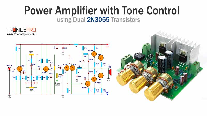
- Audio preamplifiers and tone control circuits
- Digital and analog signal amplifiers
- LED driver and logic output stages
- Sensor and detector circuits
- Pulse and waveform generator circuits
- Switching of small relays and transistors
Its small-signal design and balanced gain make it ideal for educational kits, audio experiments, and small electronic gadgets.
Working Principle of 2N5305 Transistor
The 2N5305 NPN transistor functions by controlling current flow between the collector and emitter through the base terminal. When a small base current is applied, it allows a proportionally larger collector current to pass, enabling current amplification.
In switching applications, the transistor operates between cut-off (OFF) and saturation (ON) regions. In amplification mode, it operates in the active region, ensuring linear current gain for clean signal reproduction.
Thermal and Safe Operating Conditions
To achieve maximum reliability and life span of the 2N5305, follow these precautions:
- Keep total power dissipation below 400mW with adequate ventilation.
- Maintain junction temperature below 150°C.
- Use a base resistor to limit current during input drive.
- Avoid reverse biasing beyond rated voltage limits.
- In high-frequency circuits, ensure proper decoupling and grounding.
Advantages of Using 2N5305
- Compact size fits easily into any small circuit board.
- Consistent linear gain suitable for low-level audio stages.
- Low collector-emitter saturation voltage improves efficiency.
- Low cost and easy availability for educational projects.
- Reliable for repetitive switching and pulse circuits.
Conclusion
The 2N5305 NPN transistor is a practical choice for low-power amplification and switching applications requiring compact packaging and dependable gain. With 25V voltage handling, 300mA collector current, and 400mW dissipation, it provides an excellent balance between performance and durability for signal, driver, and preamplifier circuits.
Its E-B-C pin configuration in a TO-92 package makes it easy to integrate into breadboards and compact electronic designs. For hobbyists, students, and professionals seeking a low-voltage general-purpose transistor, the 2N5305 is a solid and reliable option.
Datasheet & Pinout of 2N5305 NPN Transistor
Click the following Button to download the datasheet of 2N5305 Transistor :
More projects, You may like:
- Video Transmitter DIY Homemade FM Radio Transmitter
- Adjustable Power Supply DIY Battery Charger
- 12V-220V 500 Watt inverter DIY Homemade
- MPPT Solar Charge Controller DIY Homemade
- DIY LA4440 bass amplifier homemade
For more project and circuit diagrams, you can go through the Schematics in the main menu where you can find many interesting projects and circuit diagrams like audio amplifier circuits, voltage booster circuit, battery charger circuit and timer circuits etc., which are all beginner circuit projects. Feel free to check them out!

Thank you for visiting the article.


