Introduction
The LM358 is a dual operational amplifier (op-amp) IC integrated circuit combining two independent, high gain, internally frequency-compensated amplifiers in a single package. It was specifically designed to operate well on a single supply voltage, although it can also be used with dual (±) supplies. Because of its ability to sense voltages near the negative rail (ground) and its low power consumption, the LM358 is widely used in general analog signal processing, sensor interfaces, and mixed-signal systems
One key advantage of the LM358 is that its input common-mode range includes ground (the negative rail), meaning that one of its inputs can be as low as 0 V (in single-supply mode) without losing linearity. Its outputs also can swing close to the negative rail under proper loading. However, the output cannot swing fully to the positive rail under load, which must be considered in design.
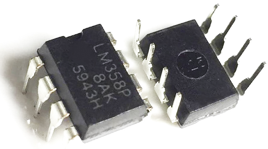
LM358 Dual Op-Amp IC
Because it is internally compensated and stable for unity gain, the LM358 is easy to use for buffers, integrators, filters, and amplifiers without requiring external compensation components. That makes it attractive for many analog designs, especially when cost and simplicity are critical. Its performance is modest in terms of speed and offset compared to modern precision op-amps, but for many low-frequency and sensor-level tasks, it remains a robust, low-cost workhorse.
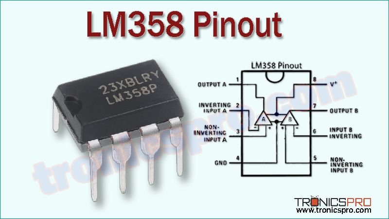
LM358 Pinout
LM358 Key Features
- Dual operational amplifiers
- Internally frequency compensated
- Wide supply voltage range
- Low quiescent current per amplifier
- Input common-mode range includes ground (negative rail)
- Output can swing close to negative rail (but not fully to positive rail under load)
- Large DC open-loop gain
- Unity-gain bandwidth
- Low input offset voltage and bias currents
- Compatible with many logic levels and suitable for interfacing with microcontroller systems
- Available in multiple package types
LM358 Specifications/Characteristics
- Supply voltage: 3 V to 36 V (B / BA versions) or ±1.5 V to ±18 V in dual-supply mode
- Quiescent current (per amplifier): ~300 µA typical (in B / BA versions)
- Input offset voltage (max): ~3 mV (for A / B versions), ~2 mV (for BA version)
- Input bias current: on the order of tens of nanoamps
- Input offset current: small, in the nanoamp range (varies by variant)
- Open-loop gain: ~100 dB typical
- Unity-gain bandwidth: ~0.7 MHz (classic), up to ~1.2 MHz (in B / BA variants)
- Slew rate: ~0.3 V/µs typical (classical version)
- Output voltage swing: can go down to (or very near) negative rail; cannot swing fully to positive rail (voltage drop ~1.5–2 V under load)
- Input common-mode voltage range: from negative rail (0 V) up to (V+ – ~1.5 V)
- Maximum output current (sink / source): limited, depending on load and voltage headroom (tens of mA in favorable conditions)
- Operating temperature range (commercial version): 0 °C to +70 °C (some versions extend this further)
- Package types: PDIP-8, SOIC-8, TSSOP-8, etc.
Note: DATASHEET DOWNLOAD button is provided end of this article.
Pin Configuration of LM358 Dual Op-Amp IC
| Pin# | Pin Name | Pin Description |
|---|---|---|
| 1 | OUT1 | Output of amplifier 1 |
| 2 | IN1 (–) | Inverting input of amplifier 1 (negative input) |
| 3 | IN1 (+) | Non-inverting input of amplifier 1 |
| 4 | V– / GND | Negative supply / ground (negative rail) |
| 5 | IN2 (+) | Non-inverting input of amplifier 2 |
| 6 | IN2 (–) | Inverting input of amplifier 2 |
| 7 | OUT2 | Output of amplifier 2 |
| 8 | V+ | Positive supply voltage input |

More Circuit Layouts


Key Applications of LM358 Dual Op-Amp IC
- Signal conditioning and amplification for sensors (thermistors, strain gauges, photodiodes)
- Voltage followers / buffers and impedance matching
- Active filters (low-pass, high-pass, band-pass)
- Summing amplifiers, difference amplifiers
- Integrator / differentiator circuits
- Oscillators, waveform generation, and nonlinear analog circuits
- Low-side current sensing (when inputs near ground)
- Analog-to-digital front-end signal scaling
- Comparator-like threshold circuits (though not ideal for fast switching)
- Battery-powered systems and portable devices (because of low quiescent current)
LM358 Equivalent ICs / Alternatives
- LM358A / LM358B / LM358BA — improved variants with lower offset and slightly better specs (drop-in)
- LM2904 — similar dual op-amp often used interchangeably with LM358
- LM224 / LM258 — related family members with similar pinouts and characteristics
- TLV2372 / TLV2374 — modern low-offset, rail-to-rail dual / quad op-amps (depending on application)
- OPA2376 / OPA2176 (or other precision dual amplifiers) — when you need better precision, lower noise, or wider bandwidth
- MCP6002 — a modern rail-to-rail dual op-amp alternative (depending on supply voltage and performance needs)
- NE5532 (dual) or TL072 (dual) — for audio / higher performance applications (though these often need ± supplies)
(The pinout for certain ICs can vary from that of the LM358).
Datasheet of LM358 Dual Op-Amp IC
Click the following Button below to download the datasheet of LM358 :
More projects, You may like:
- Video Transmitter DIY Homemade FM Radio Transmitter
- Adjustable Power Supply DIY Battery Charger
- 12V-220V 500 Watt inverter DIY Homemade
- MPPT Solar Charge Controller DIY Homemade
- DIY LA4440 bass amplifier homemade
For more project and circuit diagrams, you can go through the Schematics in the main menu where you can find many interesting projects and circuit diagrams like audio amplifier circuits, voltage booster circuit, battery charger circuit and timer circuits etc., which are all beginner circuit projects. Feel free to check them out!
Thank you for visiting the article.