The 2N4920 pinout follows the Emitter–Collector–Base (E–C–B) configuration in a TO-126 package, offering reliable performance and easy installation for medium-power circuits. The 2N4920 PNP transistor is a silicon medium-power device designed for audio amplifiers, driver stages, and regulated power supplies. With its ability to handle high voltage and current levels, it delivers consistent performance across a wide range of low-frequency and switching applications.
This transistor is known for its durability, efficiency, and strong thermal stability, making it a solid choice for use in industrial, automotive, and consumer electronic designs.

Introduction to 2N4920 PNP Transistor
The 2N4920 is the highest-voltage version in the 2N4918, 4919, 4920 transistor family.
It can withstand a collector-emitter voltage up to −80 V, allowing it to perform well in higher-voltage amplifier and switching circuits where other medium-power devices may not be suitable.
Because of its low leakage current and high gain consistency, the 2N4920 transistor is often used in class-AB amplifiers, power regulators, and push-pull output stages.
Its TO-126 package provides excellent heat dissipation, while its E–C–B pinout simplifies integration in printed circuit boards.
2N4920 PNP Transistor

Pinout of 2N4920

Understanding the 2N4920 Pinout Configuration
The 2N4920 has three terminals, arranged Emitter–Collector–Base (E–C–B) from left to right when facing the flat front side.
This orientation is widely used in power amplifier transistors, helping to ensure compatibility with existing circuit layouts.
Pin Configuration of 2N4920 Pinout
| Pin# | Pin Name |
|---|---|
| 1 | Emitter |
| 2 | Collector |
| 3 | Base |
Key Features of 2N4920 Transistor
- Designed for medium-power audio and switching applications
- High voltage tolerance ensures stable operation
- Excellent thermal efficiency with TO-126 packaging
- Provides low distortion and linear amplification
- Offers high reliability in demanding environments
- Compatible with wide temperature ranges
2N4920 Transistor Datasheet and Specifications
- Collector–Emitter Voltage (Vce): −80 V
- Collector–Base Voltage (Vcb): −80 V
- Emitter–Base Voltage (Veb): −5 V
- Collector Current (Ic): 1.0 A
- Power Dissipation (Pc): 30 W
- DC Current Gain (hFE): 30 – 180
- Transition Frequency (fT): 3 MHz (typical)
- Polarity: PNP
- Package Type: TO-126
- Pin Configuration: Emitter–Collector–Base (E–C–B)
Working Principle of 2N4920 PNP Transistor
The 2N4920 transistor works on the bipolar junction principle, where a small base current controls a larger emitter-collector current flow.
In the active region, it functions as a current amplifier, producing an amplified output signal with low distortion.
When the base voltage is more negative than the emitter, the transistor conducts, enabling efficient current control and amplification.
Because of its high collector-emitter voltage capability, the 2N4920 is particularly suited for medium-voltage driver circuits, power output stages, and linear regulators.
Its TO-126 body ensures minimal thermal stress and reliable long-term operation.
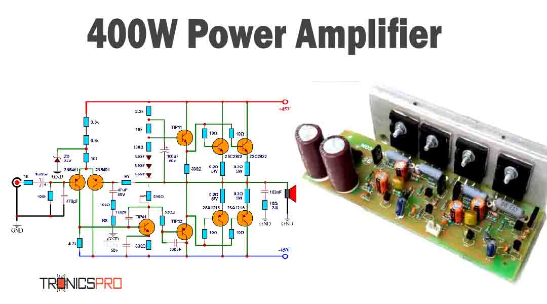
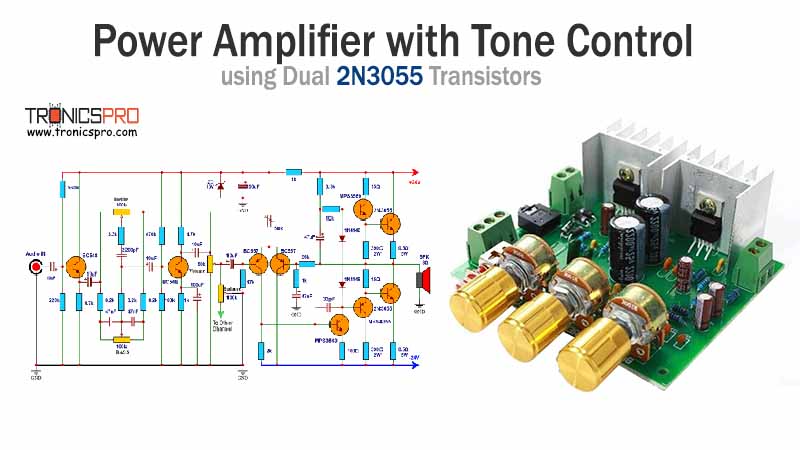
More Circuit Layouts






Typical Applications of 2N4920
- Audio power amplifiers
- Driver and output stages
- Voltage and current regulators
- Power control and switching circuits
- Signal and analog amplifiers
- Push-pull configurations
Equivalent Transistors and Alternatives
- BD242 – PNP transistor with comparable voltage and current handling
- BD140 – TO-126 medium-power PNP replacement
- TIP32C – Suitable alternative for power amplifier designs
- MJ2955 – High-current PNP substitute
- 2N2905A – Lower-current alternative for general applications
Frequently Asked Questions (FAQ)
What is the maximum collector current of 2N4920?
The maximum collector current is 1.0 A.
What is the voltage rating of 2N4920?
The transistor supports up to −80 V collector-emitter and −80 V collector-base voltage.
What is the 2N4920 pin configuration?
The 2N4920 pinout is Emitter–Collector–Base (E–C–B) when viewed from the flat face.
What is the power dissipation of 2N4920?
It can safely dissipate up to 30 W when properly heat-sunk.
What package type does 2N4920 use?
It uses the TO-126 package, known for compact design and efficient heat dissipation.
Conclusion
The 2N4920 PNP transistor offers high-voltage capability and stable performance in a TO-126 package with E–C–B pin configuration.
It is well-suited for audio amplifier outputs, medium-power switching, and voltage regulation circuits.
With its strong build, high reliability, and smooth linear operation, the 2N4920 transistor remains a preferred component for professional and hobby electronics projects that require up to −80 V operation.
Datasheet & Pinout of 2N4920 PNP Transistor
Click the following Button to download the datasheet of 2N4920 Transistor :
More projects, You may like:
- Video Transmitter DIY Homemade FM Radio Transmitter
- Adjustable Power Supply DIY Battery Charger
- 12V-220V 500 Watt inverter DIY Homemade
- MPPT Solar Charge Controller DIY Homemade
- DIY LA4440 bass amplifier homemade
For more project and circuit diagrams, you can go through the Schematics in the main menu where you can find many interesting projects and circuit diagrams like audio amplifier circuits, voltage booster circuit, battery charger circuit and timer circuits etc., which are all beginner circuit projects. Feel free to check them out!

Thank you for visiting the article.


