The BD539 NPN transistor is a powerful and reliable device designed for amplification and switching applications. Known for its high collector current and voltage handling capability, it is ideal for use in audio amplifiers, power regulators, and driver circuits. This guide explains the BD539 pinout, equivalent transistors, datasheet, and applications, helping you understand its specifications and how to use it effectively with its complementary BD540 PNP transistor.

Introduction to BD539 NPN Transistor
The BD539 NPN transistor is a high-power silicon transistor widely used in audio amplifiers, voltage regulators, and switching circuits. Known for its excellent current handling capacity, high voltage tolerance, and robust performance, the BD539 is a favorite among circuit designers who work on medium to high-power amplification projects.
With a maximum collector current (Ic) of around 4A and a collector-emitter voltage (Vce) up to 100V, the BD539 transistor delivers strong electrical efficiency and stability. It belongs to the complementary pair family, where its PNP counterpart is the BD540 transistor. Together, these transistors are used in push-pull output stages and power driver circuits for balanced signal amplification.
The BD539 transistor datasheet indicates that it features excellent gain characteristics, wide safe operating area (SOA), and low saturation voltage, making it ideal for both analog and digital circuit designs. Because of its TO-220 package, it also supports efficient heat dissipation, ensuring long-term reliability even in continuous operation.
BD539 NPN Transistor
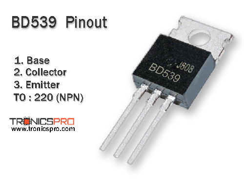
Pinout of BD539
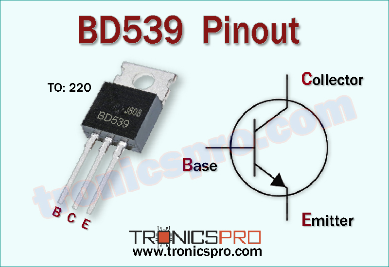
Understanding the BD539 Pinout Configuration
The BD539 pinout defines the transistor’s electrical connectivity and polarity. It helps circuit engineers correctly identify which lead connects to the base, collector, and emitter terminals. The BD539 follows a standard TO-220 transistor package, commonly used in power devices for its strong mechanical and thermal properties.
When facing the flat side with leads downward, the pin configuration is typically:
Pin 1 – Base (B), Pin 2 – Collector (C), Pin 3 – Emitter (E).
This pin layout allows simple integration in PCB designs and breadboard testing environments. Understanding the BD539 pin configuration is crucial when replacing or pairing it with its complementary BD540 PNP transistor in amplifier stages.
Pin Configuration of BD539 Pinout
| Pin# | Pin Name | Pin Description |
|---|---|---|
| 1 | Base | Controls transistor biasing |
| 2 | Collector | Connected to load/output |
| 3 | Emitter | Common terminal for current flow |
Key Features of BD539 Transistor
- High collector current handling capability
- Wide safe operating area for power circuits
- Low collector-emitter saturation voltage
- Excellent gain linearity and switching response
- Suitable for audio and driver stages
- TO-220 insulated package for better heat dissipation
- Compatible with complementary PNP transistor BD540
BD539 Transistor Datasheet and Specifications
The electrical characteristics of BD539 define its operating limits and performance in electronic circuits. These parameters are confirmed from the BD539 datasheet by STMicroelectronics:
- Collector-Emitter Voltage (Vceo): 100V
- Collector-Base Voltage (Vcbo): 100V
- Emitter-Base Voltage (Vebo): 5V
- Collector Current (Ic): 4A
- Total Power Dissipation (Ptot): 40W
- DC Current Gain (hFE): 40 to 160 (depending on Ic and Vce)
- Transition Frequency (fT): 3 MHz typical
- Operating and Storage Junction Temperature: -65°C to +150°C
- Package Type: TO-220
These characteristics ensure high reliability and efficiency in both linear and switching applications. The BD539’s low saturation voltage (Vce(sat)) reduces power loss, improving circuit efficiency, especially in high-current designs.
Working Principle of BD539 NPN Transistor
The BD539 transistor operates as a current-controlled amplifier or switch. When a small current is applied to its base, it allows a much larger current to flow from the collector to emitter. This principle forms the basis of transistor amplification.
In amplifier circuits, the BD539 boosts weak input signals, while in switching circuits, it acts as a controlled on/off gate for power delivery. The transistor remains in cutoff mode when the base is not biased and enters saturation when fully turned on, allowing maximum current conduction. Its NPN polarity means current flows from collector to emitter when the base is positively biased.
More Circuit Layouts


Typical Applications of BD539
The BD539 transistor is versatile and found in numerous industrial, automotive, and electronic consumer products. Common applications include:
- Audio power amplifiers
- DC motor drivers
- Power regulators and converters
- Switching circuits
- Output stages in amplifiers
- Inverter and control circuits
- Relay drivers and lamp controllers
Because of its high gain and current capacity, the BD539 is particularly suitable for medium-power linear amplifiers and power driver circuits where stability and efficiency are crucial.
PNP Complementary Transistor
The PNP complementary transistor of BD539 is the BD540 transistor. Together, they form a complementary pair used in push-pull amplifier configurations, providing symmetrical signal amplification with minimal distortion.
In such designs, the BD539 handles the positive half-cycle of the signal (NPN side), while the BD540 manages the negative half-cycle (PNP side), resulting in a more efficient and balanced audio output.
The pairing of BD539 vs BD540 also allows circuit designers to implement advanced driver stages in both analog and digital systems.
Equivalent Transistors and Alternatives
If the BD539 transistor is unavailable, several equivalent and replacement transistors can be used depending on voltage and current requirements. Some common BD539 equivalents include:
- 2N3055 (for higher power applications)
- BD237 / BD243 (moderate current capability)
- TIP31C (general-purpose NPN power transistor)
- MJ2955 / BD540 pair for complementary operation
Always check electrical ratings and pinout before substitution to ensure circuit compatibility.
Comparison BD539 vs BD540 Complementary Transistors
The BD539 (NPN) and BD540 (PNP) are complementary power transistors that share identical voltage, current, and gain characteristics but differ in polarity.
The BD539 NPN conducts when its base is driven positive relative to the emitter, whereas the BD540 PNP conducts when its base is negative relative to the emitter. This opposite operation allows them to work together in push-pull configurations, improving signal linearity and reducing distortion in amplifier circuits.
In summary, the BD539 handles the positive current flow, while BD540 mirrors it for the negative cycle, ensuring smooth and balanced output performance.
Frequently Asked Questions (FAQ)
What is the BD539 transistor used for?
The BD539 transistor is mainly used in audio power amplifiers, voltage regulators, and switching circuits that require medium to high current handling.
What type of transistor is BD539?
It is an NPN silicon power transistor designed for medium and high-power linear and switching applications.
What is the BD539 pin configuration?
The BD539 has a TO-220 package with pin configuration: Pin 1 – Base, Pin 2 – Collector, Pin 3 – Emitter.
What is the complementary transistor for BD539?
The complementary PNP transistor for BD539 is BD540.
Can I use BD238 instead of BD539?
No, BD238 has lower voltage and current ratings compared to BD539. It is not recommended as a direct substitute unless circuit power requirements are low.
Conclusion
The BD539 NPN transistor is a reliable and powerful component suitable for medium to high-current applications. Its robust design, broad safe operating area, and high efficiency make it a preferred choice for audio amplifiers, regulators, and power control systems. When paired with its complementary BD540 PNP transistor, it offers balanced amplification and smooth performance in complex electronic circuits.
For circuit designers, understanding the BD539 pinout, datasheet values, and equivalents ensures proper implementation and maximum performance in real-world electronic designs.
Datasheet of BD539 NPN Transistor
More projects, You may like:
- Video Transmitter DIY Homemade FM Radio Transmitter
- Adjustable Power Supply DIY Battery Charger
- 12V-220V 500 Watt inverter DIY Homemade
- MPPT Solar Charge Controller DIY Homemade
- DIY LA4440 bass amplifier homemade
For more project and circuit diagrams, you can go through the Schematics in the main menu where you can find many interesting projects and circuit diagrams like audio amplifier circuits, voltage booster circuit, battery charger circuit and timer circuits etc., which are all beginner circuit projects. Feel free to check them out!
Thank you for visiting the article.
You may also like:
![2SC1815 NPN Transistor Datasheet Pinout]()
2SC1815 NPN Transistor Datasheet Pinout
![2SD882 NPN Transistor Datasheet Pinout]()
2SD882 NPN Transistor Datasheet & Pinout
![BC556 PNP Transistor Pinout Datasheet]()
BC556 PNP Transistor Pinout Datasheet
![BD433 NPN Transistor Datasheet]()
BD433 NPN Transistor Pinout Datasheet
![2SB688 PNP Transistor Datasheet Pinout]()
2SB688 PNP Transistor Datasheet & Pinout
![BC638 PNP Transistor Datasheet]()
BC638 PNP Transistor Pinout Datasheet
![C5200 NPN Transistor Thumbnail]()
2SC5200 NPN Transistor - Datasheet
![BD240 PNP Transistor Datasheet]()
BD240 PNP Transistor Pinout Datasheet